On a different note
At the risk of over stating the obvious, I think this would make a pretty good multi-channel home theater amp.
Especially since it only needs one transformer per 2 channels and the heat sinks need not be so huge.
Once boards are available, I bet a few will build it as such.
At the risk of over stating the obvious, I think this would make a pretty good multi-channel home theater amp.
Especially since it only needs one transformer per 2 channels and the heat sinks need not be so huge.
Once boards are available, I bet a few will build it as such.
Re: On a different note
As Al used to say with respect to heatsinks for this amplifier "You need bigguns"
(That's from "Married with Children").
It's like 0.8 C/W -- or like a 36C kind of heatsink.
vdi_nenna said:At the risk of over stating the obvious, I think this would make a pretty good multi-channel home theater amp.
Especially since it only needs one transformer per 2 channels and the heat sinks need not be so huge.
Once boards are available, I bet a few will build it as such.
As Al used to say with respect to heatsinks for this amplifier "You need bigguns"
(That's from "Married with Children").
It's like 0.8 C/W -- or like a 36C kind of heatsink.
Yeah, I guess you're right. They'd be biggums alright. One would have to love big amps to build something that enormous. 😉
A multi-ch. amp doesn't need to join the heatsinks at the hip like e.g. an Aleph-5, so you can get away with fairly small heatsinks, for example the familiar and cheapo 9-flange SK53 type.
Still a double or triple D-cup, but no bigg'uns.
(Hands Up who likes to hold a weenie during TV watching and dream of the shoe sale racket.)
Still a double or triple D-cup, but no bigg'uns.
(Hands Up who likes to hold a weenie during TV watching and dream of the shoe sale racket.)
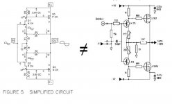
Back to the feedback network in the f5. Looking at the more triditional method on the right for the moment neglecting the
common feedback resistor. Distortion in one jfet will be injected
into the other one by the voltage developed across r15 giving
a push pull distortion signiture. So we have a pushpull front
end runing a push pull output stage.
But in the f5 the front end is operating as a pair of single devices
this is powering the push pull output stage.
Hay I could be wrong but like the girl in the song said "at least I
an't drinking"
Attachments
woody said:Back to the feedback network in the f5. Looking at the more triditional method on the right for the moment neglecting the
common feedback resistor. Distortion in one jfet will be injected
into the other one by the voltage developed across r15 giving
a push pull distortion signiture. So we have a pushpull front
end runing a push pull output stage.
But in the f5 the front end is operating as a pair of single devices
this is powering the push pull output stage.
Hay I could be wrong but like the girl in the song said "at least I
an't drinking"
yup - that's exactly the point - in F5 each input jfet can't see and feel another one ;
they are diff amplifier , but not LTP ;
Papa probably tested each variant , and decided/implemented what's more kinky

devil is in details , we agree on that already

Zen Mod said:in F5 each input jfet can't see and feel another one
Not entirely true.
jacco vermeulen said:
Not entirely true.
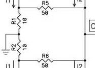
lay dawn and make me 100 push -ups , ya cwayzee dutchie ;
then look at your hands , fists , whatever you use to make push-ups ( thumbs , even ) ;
is ground closer to each hand , than hand to hand ?
in any case , ground is closer than 50+50 route............... and considering that you already have big-bang where + is situated in equitation .......
Attachments
I think I found (by simming my a** off) one significant reason for that specific feedback arrangement:
Compared to the conventional hookup the open loop gain can be made a little higher, all else being equal -- all DC/large-signal operating points, output loading from the feedback network (I missed this one in the last try a while back) and closed-loop gain. Now when I look at it is rather obvious, the path to GND from either source can be made "better" without increased load for the output and thus without increased dissipation in the network. Looks like the best possible way of implementing a low impedance feedback with least negative side effects.
Consequences are lower output impedance and more error feedback, producing less distortion. But the differences aren't that big, in my simulation, all within a +-5% margin (also for the various distortion profiles). When I inject a noise pulse in the MOSFET gates, there is ~30% less feedthrough at the output, and when I drop the AC open loop gain with series RC's across the I/V-resistors (R3, R4 in the simplifed circuit) to get the same open loop gain the feedtrough is the same. This seems to fit the ~2dB more loop gain I roughly figured out.
Other differences, again Nelson's arrangement looking better overall, are distortion under very heavy class-B excursion, and voltage clipping behaviour. I found the single-ended vs. push-pull considerations and their distortion consequences only a minor issue, but probably there is also something to that.
- Klaus
FWIW, now I just noted some small error in the published simplified schematic, a typical cut&paste mishap: R4 should be 600R (or so) not 0.47R
- Klaus
- Klaus
KSTR said:FWIW, now I just noted some small error in the published simplified schematic, a typical cut&paste mishap: R4 should be 600R (or so) not 0.47R
Klaus, Patrick was a bit quicker than you 😀
http://www.diyaudio.com/forums/showthread.php?postid=1482312#post1482312
Tino
Yes Tino,
some 57 pages quicker
BTW, additional footnote to my sims, the gm's of K170 and J47 are both ~40mS (@Id=~10mA) for the parts I used. In the article, 20mS is quoted.
- Klaus
some 57 pages quicker
BTW, additional footnote to my sims, the gm's of K170 and J47 are both ~40mS (@Id=~10mA) for the parts I used. In the article, 20mS is quoted.
- Klaus
> Klaus, Patrick was a bit quicker than you
Just a bit ...... 🙂
> additional footnote to my sims, the gm's of K170 and J47 are both ~40mS (@Id=~10mA) for the parts I used. In the article, 20mS is quoted.
At Id=6mA, 2SK170BL has a Yfs of about 33mS, and 2SJ74BL about 40mS, according to the some 400 examples that I have measured.
i.e. the transocductances are NOT the same.
Regards,
Patrick
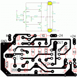
Re: PCB
Yes, but then the input FETs won't be facing each other for better thermal coupling. Jumper may be avoided by moving drain lead from input J74 through 200 R pot, but that's unelegant.
There are situations when jumper just makes more sense 😉
estman said:Hi Juma,
you may want to turn inp. 2sj74 180deg, so we get rid of jumper 😉
Yes, but then the input FETs won't be facing each other for better thermal coupling. Jumper may be avoided by moving drain lead from input J74 through 200 R pot, but that's unelegant.
There are situations when jumper just makes more sense 😉
- Home
- Amplifiers
- Pass Labs
- F5 power amplifier