Wow, very interesting.
But I don't get this (even what do you mean by "The thermal drop in the sink to insulator grease will be over twice as much with the thin mica than the alumina."
Do you mean that grease + mica = better conductivity vs grease + AlO or the opposite?
Thanks !
The Al203 is better because it make the heat spread out more at the heatsink interface. That reduces the thermal drop at that layer, whereas the very thin mica will not allow as much spread.
edit: in the example numbers I provided, the mica provided an 8mm by 8mm area for heatflow, or 64 square mm, and the 2mm thick alumina gave a 12mm by 12mm area, or 144 square mm.
144/64 = 2.25, the ratio.
If there is a one degree C per watt thermal drop in the grease under the thin mica, there will be a .44 drop under the alumina.
jn
Last edited:
The transistor is not shooting heat balls or something, heat travels omnidirectional. True that the hot area gets larger with distance but the pyramid is nonsense. Think of it more like a bubbleThis is a pic from a google search. (only the left drawing) Note that the heat travels roughly in a pyramidal fashion.
Heat "travels" through a path of least resistance. Idealy it could be omnidirectional. The area refered to as omnidirectional that is outside the pyramid is trying to travel to the air. Not a low Rth path at all. Not traveleing much. The path of greatest thermal conductivity is what the analogy is pointing out. However, feel free to show us your ideas on an omni directional heatsink device 😉
I'd think that a real power transistor has a lead frame inbetween die and insulator, with a thermal conductivity that far outruns any insulator material type.
In practice, one would require an insulator of a larger size than the footprint of the power device.
And even then, there's the law of diminishing returns.
At 2mm off center, effective thermal resistance would be 41% higher.
At 4mm off center, it would have gone up ~124%.
Works for large-die Zetex sot223 devices though.
Attachments

Last edited:
The transistor is not shooting heat balls or something, heat travels omnidirectional. True that the hot area gets larger with distance but the pyramid is nonsense. Think of it more like a bubble
You need to learn a tad more about the topic. I recommend you google 45 degree heat spread model before spreading more incorrect information.
1. Heat will indeed travel isotropic if it is being generated at the center of a uniform mass. Transistors are NOT that. They are planar devices typically .025 inches thick, power devices range from .1 inch by .1 inch out to .5 inches square (general consumer devices of course, not the hockey puck compression devices 2 and 3 inches in diameter that I am used to using). They are dissipating their heat onto a flat planar surface, eliminating one half of the "spherical" isotropic heat path.
2. Typical power semiconductors are mounted onto a copper, aluminum, or steel baseplate that will range from .03 inches to .08 inches thickness. As a consequence, even a hemispherical heat wavefront will immediately hit a thermal interface, that being the bottom of the package. If the thermal conductivity at that interface could be in the metal range, like copper or aluminum, and sufficiently sized, the hemispherical wavefront could continue. However, it never is. So you are left with a very thin section of conductive metal placed on top of a relatively poor thermally conductive material.
3. As the heatfront travels laterally in the baseplate, it continues it's decline of flux density, and becomes less a contributor to flux through the thermally insulating barrier. As a consequence, the farther from under the die you get, the less the contribution to the overall thermal path conductivity the material becomes.
The result of all this? To gain an exact model of the thermal resistance of a packaged device mounted to a heatsink, one can use ansys or some other modeling technique. The beauty of large modellers like ansys is the ability to also examine the Von Mises stresses in the die to bottom solder joint. This comes in handy with military hardware which needs to pass thermal cycling (or power cycling), but again is of little use to the diyer.
The 45 degree model for heat transport was developed to easily model the heat transport for power semi's in descrete form as you will use, and in the hybrid form as I've built and tested in the past. While it does make some assumptions of flow path (which you don't like), it does indeed produce results consistent with reality at the 2 to 4% error level. As such, it is very easy for even professional designers to get VERY close to reality in thermal modeling of power devices.( edit: it is of note that die thermal resistance values can have a larger spread of variation as a consequence of the die attach process, where voiding at the interface can create hotspots which crowd the dissipation to an effectively smaller chip area, or cold voids which remove a portion of the active die from the dissipation by starving the current path in the silicon. In addition, variations in package, insulator, and heatsink texture and thermal grease thickness variations will impact the final real world result, so trying to model to the .5% level is an exercise in futility.(pretty much like my ability to spell))
The ONLY weak point in the 45 degree model is the accurate portrayal of the spread angle above very large discontinuities in thermal conductivity. In the limit, the surface above a thermal insulator will go isothermal, effectively widening the spread angle above the discontinuity. My spreadsheet includes the option of setting the angle, but it does not automatically calculate it since I choose to never use bad thermally conducting materials to cool power semi's.
From my experience in designing, building, and thermally testing heat transport effectiveness in power semiconductors, I find the 45 degree model to be very good at providing predictions of thetaJC.
By far, the best aspect of the model is the "what if" capability for immediate feedback of material and design choices. What if I replace a .001 inch mica with a .025 inch alumina, what if I replace the .002 inch grease layer with a .005 mil thick layer of pyrolitic graphite?
I recommend you research the topic if you wish to engage further. Ask questions if you wish, I can easily answer them.
jn
PS...my apologies for using inches, I have yet to convert my article or spreadsheet to metric units, and have not committed the metric sizes to memory, which is what I used for this post.
Last edited:
Hello,
New to diyAudio and hope I'm posting in the right place.
I had a question that I wanted to put out there for any folks who have cascoded any of their F5s. In the V3 schematic the negative rail has a 47.5K resistor at R26 while the positive rail has a 10K resistor at R25. Unless i'm looking at something very wrong this gives rise to about +9.4V to the 2SK170 and about -2.4V to the 2SA1837. Should these be equal?
I'm assuming this value is correct as this is an awesome amp that has been reproduced so many times by folks on this site. I'm just trying to wrap my head around the cascode values here.
Thanks for any help!
47K5 for R26 is a typo. Make it 10K, like R25. Nobody is perfect, although Nelson Pass comes close.
On the picture to the left I see a heatsink with infinite length?google 45 degree heat spread model

If you can calculate stuff with your linear model with a defined error, great, but I hate these "diagrams" being shown as if they were some image of reality ... that must be misleading and then they are as such nonsense. No? Nevermind ...
Last edited:
As I said, the picture on the left simply depicts the 45 degree path between a dissipator on the top surface, and the bottom surface. The picture on the right shows the pyramid shape of the heat flux pattern used in the model.On the picture to the left I see a heatsink with infinite length?
If you can calculate stuff with your linear model with a defined error, great, but I hate these "diagrams" being shown as if they were some image of reality ... that must be misleading and then they are as such nonsense. No? Nevermind ...
It would have been easier to show the model using my own diagrams, but I was not at the computer with the drawings.
The 45 cone can be considered as reality, as it very closely mimics the actual heat flow path. So well, that it is trivially easy to determine the impact lower layer materials will have on the final outcome. Any loss in fidelity of the model because it's not a full blown FEA is countered by the ease of creating a valid model using an excel spreadsheet which provides results within milliseconds instead of a long iterative analysis.
Calling it nonsense because you do not understand it serves no useful purpose. A little more scientific rigor would be welcomed.
By the way, you calling it a heatsink of infinite length is interesting in itself. The drawing clearly is not that, but your statement indicates that you understand that the model does not consider material outside the cone, so does indeed express the indication that an infinite sink would not impact the model. You do have good intuition from what I see.
jn
Last edited:
47K5 for R26 is a typo. Make it 10K, like R25. Nobody is perfect, although Nelson Pass comes close.
keeping these mistakes at pretty same level , just to be sure that Greedy Boyz are having brains in ON state

NO ! NO ! NO !just go for it
prior to powering up , back up with trimpots to zero bias (confirm min. pot value with ohmmeter across R5,R6 !!) , ....................
Don't just go for it.
Set P1 and P2 to zero ohms. Check with an ohm-meter.
Set P3 to mid value. Check with ohm-meter.
THEN "go for it" using a bulb tester to power ON and check voltages are as expected. If all OK
Remove bulb tester and power ON direct to the Mains. Start adjusting bias with P1 and P2 as explained in the build guide. Do not adjust P3, it remains at mid value.
Last edited:
Temp measurements
I too wondered about the convection effect. Thanks for testing and sharing the results.
I noticed you have 3 temp probes setup: 1 taped to a heatsink on the workbench and 2 taped to each channel's heatsink. Are these K-type connected to a DMM or did you make your our with thermistors?
I too wondered about the convection effect. Thanks for testing and sharing the results.
I noticed you have 3 temp probes setup: 1 taped to a heatsink on the workbench and 2 taped to each channel's heatsink. Are these K-type connected to a DMM or did you make your our with thermistors?
I verified my conjecture about the chimney effect of the heatsinks mounted fin-to-fin in my F4 amplifier. Each channel is biased to 1.36A with 22.6V rails for a total of about 125W total dissipation. I measured ambient and heatsink temperatures for two configurations: fin-to-fin and fins outward as shown in the photos. The temperatures shown were after more than one hour and were stable.
fin-to-fin fins-outward
ambient: 20.1C 20.1C
left channel: 42.3C 44.9C
right channel: 42.3C 44.9C
<sorry - I cannot figure out how to present a table with this "editor">
I too wondered about the convection effect. Thanks for testing and sharing the results.
I noticed you have 3 temp probes setup: 1 taped to a heatsink on the workbench and 2 taped to each channel's heatsink. Are these K-type connected to a DMM or did you make your our with thermistors?
Did the wood come into play? If I read it correctly, when the wood was being used the temps were higher.
jn
Thermistor - sperm like
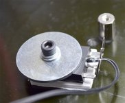
Hello,
I have these thermistors that are black, a dot and 2 flexible leads. Because the leads are flexible I have glued the thermistor end to the center pin of the FET. However the leads look flimsy.
Should I worry about the leads and heat. I used Arctic White Epoxy Thermal Glue.
See image attached....
Thanks.
Attachments
Nice work. I wouldn't worry about the leads too much, but you might want to twist them lightly.Hello,
I have these thermistors that are black, a dot and 2 flexible leads. Because the leads are flexible I have glued the thermistor end to the center pin of the FET. However the leads look flimsy.
Should I worry about the leads and heat. I used Arctic White Epoxy Thermal Glue.
See image attached....
Thanks.
I liked your idea of the washer to spread force. However, that will not accomplish placing the force where it is the most effective. The best place to put all the force is the geometric center of the package, where the mounting hole isn't (of course). As it is, the washer is only raising the screw head, it doesn't transfer the force to the package center.
I'd tap the sink on both sides of the package, and use a bar across the device to put force in the middle. In addition, I'd pre-bend the bar into a curve, and use it concave side up so that as you tighten the side screws, the bar will tend to flat. As an alternate, you could put a small bellville on the package cup side down, and the bar will apply force central to the package.(put a flat washer under the bellville so that the force is not limited to the package edges).
Uniformity in pressure is your friend.
jn
Did the wood come into play? If I read it correctly, when the wood was being used the temps were higher.
jn
Good point. Less aluminum to dissipate heat, makes sense. So the fins facing each other didn't make much of a difference after all?
Thanks for the tips!
But I need to run it first as is with the washers. Besides, those pads are Alu Oxide so they don't take much pressure before they break. And the DIY store is 'moving' so nothing otherwise to use other than Mica which is boring. I'll have to see what kind of temperatures I get. The sinks are 0.30C/Watt so should be 'just right'.
But I need to run it first as is with the washers. Besides, those pads are Alu Oxide so they don't take much pressure before they break. And the DIY store is 'moving' so nothing otherwise to use other than Mica which is boring. I'll have to see what kind of temperatures I get. The sinks are 0.30C/Watt so should be 'just right'.
Nice work. I wouldn't worry about the leads too much, but you might want to twist them lightly.
I'd tap the sink on both sides of the package, and use a bar across the device to put force in the middle. In addition, I'd pre-bend the bar into a curve, and use it concave side up so that as you tighten the side screws, the bar will tend to flat.
Uniformity in pressure is your friend.
jn
Attachments

- Home
- Amplifiers
- Pass Labs
- F5 power amplifier