yes you could operate it with supplies from +/-15V to +/-30V.
I thought you might have something else to say (something a bit more interesting).
I thought you might have something else to say (something a bit more interesting).

yes you could operate it with supplies from +/-15V to +/-30V.
nope +/-30 V
be responsible claiming again what's wrong .
we all make mistakes ( especially me
 ) , but seeing them is important
Don't believe everything you read in a spec sheet.
I have been doing this for some time now without problems.
I think Nelson even occassionally pushes them to this level or higher in this type of topology.
Having said that, I agree I should have stated that using +/-30 V is starting to push the limits of this device.
I have been doing this for some time now without problems.
I think Nelson even occassionally pushes them to this level or higher in this type of topology.
Having said that, I agree I should have stated that using +/-30 V is starting to push the limits of this device.
Last edited:
Here is a quote from the man himself
I routinely push these parts to as high as 40V in my own
stuff. They seem to have been spec'd at lower voltage for
Gate current. If you can put up with higher Gate current,
then you'll find them actually breaking down around 42-43 V.
Not that I recommend that you build an amp on this
assumption...
And has no one mentioned cascoding these?
😎
read Pass again.
They are breaking down >=43V.
You have 30Vdc +-AC output.
You could easily have 55V across the output FETs.
Now look at output bias for the ClassA output current your load wants/needs.
What is the FET quiescent power dissipation?
They are breaking down >=43V.
You have 30Vdc +-AC output.
You could easily have 55V across the output FETs.
Now look at output bias for the ClassA output current your load wants/needs.
What is the FET quiescent power dissipation?
Yes, I understand all that.
And I agree.
I assumed umut1001 also understood all of that. So I left out all of the warnings, I probably should have addressed.
As I said before I haven't had any problems doing this.
And I agree.
I assumed umut1001 also understood all of that. So I left out all of the warnings, I probably should have addressed.
As I said before I haven't had any problems doing this.

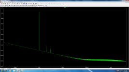
Just in case anyone is interested, here is fft of the first one.
Appologies to everyone. I won't contaminate this thread any further.
Edit: the circuit can be optimised further with changes to some resistor values eg reduce source resistors to 50 Ohms
Appologies to everyone. I won't contaminate this thread any further.
Edit: the circuit can be optimised further with changes to some resistor values eg reduce source resistors to 50 Ohms
Attachments
Last edited:
The fft looks fantastic, 2nd ~-125dB and 3rd ~-135dB and no other detected harmonics.
I wonder what the real circuit does?
I wonder what the real circuit does?
I will definitely take that as a compliment from you.
Yes it does look good.
I haven't built it so can't comment on the real world performance, but it is definitely one of the better circuits I have managed to put together (more luck than anything else, and I suppose a lot of persistance helps).
Yes it does look good.
I haven't built it so can't comment on the real world performance, but it is definitely one of the better circuits I have managed to put together (more luck than anything else, and I suppose a lot of persistance helps).
The first one simulates better, but who knows which one sounds better without actually building them.
It looks interesting!
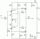
But it is not very far away from a JC-2, isn't it?
An externally hosted image should be here but it was not working when we last tested it.
the j49 in the schematic should be j74.But it is not very far away from a JC-2,
j49 is a high power Lateral mosFET.
not very far away from a JC-2, isn't it?
Depends, JC-2 Old or JC-2 New ?

read Pass again.
They are breaking down >=43V.
You have 30Vdc +-AC output.
You could easily have 55V across the output FETs.
Perhaps there is some confusion. The 43V breakdown is for
the input Jfets, which will typically not see more than the
value of a single rail voltage plus a couple volts. As a
concept, you could consider +/-40 volt rails.
We are, after all, FAB
(Fearless Amplifier Builders)
😎
Nelson,
post696 shows the same devices used in the input as in the output.
I thought a push pull stage stresses the output devices with near rail to rail voltage when driven hard.
post696 shows the same devices used in the input as in the output.
I thought a push pull stage stresses the output devices with near rail to rail voltage when driven hard.
Hi Andrew
Will 4V rms out into 100k load constitute being driven hard?
At what point do you think this will happen?
Will 4V rms out into 100k load constitute being driven hard?
At what point do you think this will happen?
It looks interesting!
But it is not very far away from a JC-2, isn't it?
An externally hosted image should be here but it was not working when we last tested it.
I haven't built or tried to simulate that one. Do you feel it is a much better solution?
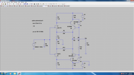
Umut wanted something that more closely represented the F5 topology in a preamp, but he asked for bipolars at the output, so that is what I tried to do. So the inspiration comes from Nelson's F5 and his paper on Cascode Amplifier Design http://www.firstwatt.com/pdf/art_cas_amp.pdf
Last edited:
... F5 topology in a preamp, but he asked for bipolars at the output...[/url]
Here you go - two versions, I like the second one more, but it's subjective. Both are easy and unexpensive to try...
Attachments

- Home
- Amplifiers
- Pass Labs
- F5 Listening Impressions & Discussion