Patrick : I asked about lowering the big electrolytic caps earlier (to be able to use salas shunts, which i have at home already), and was told that the circuit needs them to be stable.. Then why aren't they included on the veroboard design?
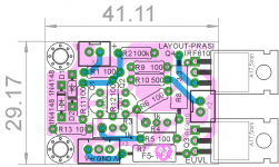
As per pcb layout on post 775, you could easily shorten the distance between R6 <-> Q4 gate by moving R6 underneath R8 (couyld move that one lower too)
You can use the leads on the resistors as direct connections between components and not need some of the tracks at all, especially some of the top layer ones
The 3 tabs for the IRF transistors don't need to be in line at all - there's no problem bending the 3 legs to different lengths for asymmetrical (?) holes
X2 connector can have right angle bent pins and be soldered from the top or bottom - same thing with R12 as it too can be mounted underneath so the 2 jfets can be bent to touch each other for temp
I'd be a bit inclined to separate the input gnd track and the output gnd connection (X2, pin 2 - you could maybe swap the pin 1 for pin 2, etc)
If you were so inclined, you could add a ground plane too altho not sure what advantage you could expect
just my 2 cents ....
Curiously, on my last amp I cut most of the pcb tracks and used mainly component leads for wiring (track pads used for mounting) - not at all surprised by a clearly better sound, in my opinion anyway!
Thanks for your suggestions, James
As per pcb layout on post 775, you could easily shorten the distance between R6 <-> Q4 gate by moving R6 underneath R8 (couyld move that one lower too)
Provided a seperate pad near the mosfet pin, so that resistor can be connected from the bottom. Anyway, as it is, the resistor pad is just 8-9mm away from the mosfet pin🙂. it just looks to be on the other side town in the zoomed-in/ magnified image of the PCB.
You can use the leads on the resistors as direct connections between components and not need some of the tracks at all, especially some of the top layer ones
The 3 tabs for the IRF transistors don't need to be in line at all - there's no problem bending the 3 legs to different lengths for asymmetrical (?) holes
I like to stick to the standard packages in my software, as drawing a new library package for every layout is not feasible.
X2 connector can have right angle bent pins and be soldered from the top or bottom - same thing with R12 as it too can be mounted underneath so the 2 jfets can be bent to touch each other for temp
X2 is a 2.54 mm pitch JST connector/ PCB header and connected from top when the mosfets are inserted from bottom., If MOSFETs are inserted from top, direct wires could be soldered or normal 2.54 mm PCB headers could be used instead of JST connector.
Yes, thats the idea behind placing the R12 resistor in between the JFETS, even when its on top side, JFETS can still be bent and coupled.
I'd be a bit inclined to separate the input gnd track and the output gnd connection (X2, pin 2 - you could maybe swap the pin 1 for pin 2, etc)
Done..
If you were so inclined, you could add a ground plane too altho not sure what advantage you could expect
I do not prefer ground plane around the pads of components, as you can see, for both the gnds, there already a plane but its contour is controlled so that it does not go around any pads.
xrk, here are the gerbs,
prasi
Attachments
Thanks, Prasi.
Looks excellent.
X
Btw, is that lion your board logo? 😎
you'r welcome
and yea its a lion😀.
Attachments

you'r welcome
and yea its a lion😀.
Hi Prasi,
Sorry to be a pain but the Gerber file seems to be missing the board outline as the PCB fab house is complaining about the Gerber file. It might be mistaking the drawing of the MOSFET for the outline of the board? Can you please check when you get a chance?
Thanks,
X
gerbs are fine. tell them to take outline / dimension layer from any of following the *.gbl *.gtl or *.gbs.Hi Prasi,
Sorry to be a pain but the Gerber file seems to be missing the board outline as the PCB fab house is complaining about the Gerber file. It might be mistaking the drawing of the MOSFET for the outline of the board? Can you please check when you get a chance?
Thanks,
X
if its pcbway, you can chat with them and tell them.
prasi
Thanks for checking Prasi.
revised silk, as cam processor converted all the font to vector graphics.
Attachments

PCBs ordered. These cute little guys and some P2P PSU modules should shrink size of amp to let me put in a 2107 case. I will probably order a dual 10w Antek 0115 toroid for a super compact PSU dual mono setup.
If anyone is interested in really shrinking the PSU, I just saw Nichicon SMT caps 1000uF 25v in 10mmx10mm SMT format. That is tiny (but expensive).
http://www.mouser.com/ProductDetail/Nichicon/UCV1E102MNL1GS/
http://www.mouser.com/ProductDetail/Nichicon/UCV1E102MNL1GS/
PCBs ordered. These cute little guys and some P2P PSU modules should shrink size of amp to let me put in a 2107 case. I will probably order a dual 10w Antek 0115 toroid for a super compact PSU dual mono setup.
Hi, xrk
Just curious whether you might have a set of this PCB to spare. I'll be more than happy to pay for them (not too expensive I hope 😛). Thanks!
Regards,
Hi, xrk
Just curious whether you might have a set of this PCB to spare. I'll be more than happy to pay for them (not too expensive I hope 😛). Thanks!
Regards,
Ok - you got the last ones. Just sent you PM. I knew I should have ordered more. They went fast.
Hi X,
I see that you don't have any PS filter cap on the pcb, are you planing to add SMD e-caps to the bottom of the board or just connect directly to the cap multiplier?
Regards
I see that you don't have any PS filter cap on the pcb, are you planing to add SMD e-caps to the bottom of the board or just connect directly to the cap multiplier?
Regards
Hi X,
I see that you don't have any PS filter cap on the pcb, are you planing to add SMD e-caps to the bottom of the board or just connect directly to the cap multiplier?
Regards
I'll have some excellent quality 5mm x 5mm boards in about 10 days that will have provisions for PS decoupling caps and will also have greater component spacing for easier soldering.
If interested, PM me.
Hi X,
I see that you don't have any PS filter cap on the pcb, are you planing to add SMD e-caps to the bottom of the board or just connect directly to the cap multiplier?
Regards
I will solder directly to bottom side of board.
revised silk, as cam processor converted all the font to vector graphics.
Very nice design but I think it needs decoupling of the trails as silently introduced in post 40. Was asking this once in the original F5 thread and got a reply that it is worse to decouple it being a "high bandwidth device" ?!?!? Found that decoupling gave better results so a load of **** that was echoed for a while.
Please add SMD 1210 (or TH) decoupling caps to the board. A 5 mm (film) input cap would be nice too. Better a slightly larger but complete board than a small board with parts dangling in the air 😉 Since its purpose seems to drive headphones or to be a preamp I think the icing on the cake would be a stereo board with pads for volume control and a muting relay. And a PSU board and ... 🙂
Last edited:
- Home
- Amplifiers
- Pass Labs
- F5 Headamp ?