With sufficient heat it will flow to both sides. I do check that I've got a fillet on both sides, and resolder if necessary.
But I'll admit that, like Gyuri, I'm potentially old-school....
But I'll admit that, like Gyuri, I'm potentially old-school....
Well I for one do appreciate you and Gyuri sharing your knowledge and experience. For all I know all my joints are weak and get hot. The bias on my F3 is barely over 1.3A so if it's not the Vgs of the LUs, what else could it be.
The problem turned out to be P1 trimpot that was stuck in a dead-short position. Replaced the pot and the channel is happy.Good day friends. What would be the cause of gross distortion on an F3 if all the parts check out? P1 and P2 does not resolve the distortion no matter how I adjust them. The LU1014 has me worried.


pretty much irrelevant
I have same numbers of Dud trimpots from Bourns and Chinese factories
pretty much 1pc per 300 or so
as long as there is Cermet inside, I don't care for name
I have same numbers of Dud trimpots from Bourns and Chinese factories
pretty much 1pc per 300 or so
as long as there is Cermet inside, I don't care for name
I suppose when you look at it that way. Still, when I buy 1 of a name-brand I expect it to work. Full stop.
But maybe it's my expectation that needs adjustment....
But maybe it's my expectation that needs adjustment....

Hi
Do the 3 MOSFET need to be matched? I’m asking because I already have enough for 2 channels (6x) but they aren’t matched.
Thanks
Eric
Do the 3 MOSFET need to be matched? I’m asking because I already have enough for 2 channels (6x) but they aren’t matched.
Thanks
Eric
Modifying F3 feedback
So, I hear some screeching from one channel of my F3 when testing for hum under a light load (headphone hum detector, ~18 ohm load on the 'LOUD' setting), but not a very light load (~166 ohms, headphone hum detector on the 'Quiet' setting). I don't know what it is but it's got a decay to it like a time constant. I'm thinking it's derived from the Aleph CCS, and it modulates whether the inputs are open (high decaying screech) vs. loaded with a source (duller deep pulses). I wonder if this is so-called oscillation, and it's got me wondering about the feedback circuit, as well as a gate stopper on the JFET.
It seems that film caps are preferred in the signal path. I don't know if the feedback loop is considered signal path or not, but the 33pF cap I'm using for position C9 is mica. The Aleph 30 build specs a 10pF mica 'compensation cap' in a similar position.
I can't tell if C9 is functioning as a high pass or low pass filter. It's described in the Zen v9 document as providing 'compensation that makes the square wave look good' which reads to me like it's meant to reduce ringing/oscillation, so low pass? If I wanted to reduce the amplifier's bandwidth to try and get rid of the screech/oscillation, what is the R to use in the RC filter calculation here? is it the 47.5K of R2 or the gate resistance of the JFET? Or something else? If a higher capacitance value here is worth trying, what value should I try? I have some nice WIMA 1uF film caps.
Edit: adding the screech
https://drive.google.com/file/d/1UnW5DdtIkgtUE1Z98Konm8cvsFy_dtgK/view?usp=sharing
Attachments

I'm a bit out of my depth here, but I don't think I'd characterize C9 as either high pass or low pass. It's for phase compensation to keep the feedback from getting 180-degrees out of phase (at which point you get runaway gain).
Thanks JeffYoung. I assure you I am way farther out of my depth.I'm a bit out of my depth here, but I don't think I'd characterize C9 as either high pass or low pass. It's for phase compensation to keep the feedback from getting 180-degrees out of phase (at which point you get runaway gain).
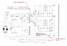
More fun. I can measure 8mV of potential difference between either channel's circuit ground and safety/earth ground, so I'm inferring I have a substantial ground loop. Would the addition of a ground lift (the pair of anti-parallel diodes shown in the schematic below) between the PSU ground of the power supply and earth ground be an acceptable mitigation?
Edit: should add, this is 8mV of DC, with the positive end on circuit ground and negative end on earth ground. I don't recall measuring for AC.
Edit: should add, this is 8mV of DC, with the positive end on circuit ground and negative end on earth ground. I don't recall measuring for AC.
Attachments
Hi
Not really a specific question for the F3 but it’s my first time working with a UMS PCB/Heatsink, I’m building an F3 from the nice CSample pcb, Issue; I’m used to always centering my MOSFET so the heat spread evenly across the entire heatsink surface. Should I go through the trouble of installing my MOSFET far apart like on my picture or will it be ok spacing them only 40mm like on a UMS pcb/heatsink? I have a feeling that I’ll have some hot spot if I don’t spread them evenly... is it paranoias??
Thanks
Eric
Attachments
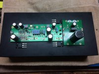
Eric it is fine. Just install like PCb shows, most of the heat is on q2. I used mica and goop on that one
Hi Chas,Matching R5 and Q1
Looking for confirmation if I did this right or not:
I tried measuring the Vgs using the circuit in image below and then choosing R5 based on the chart, but taking the Vgs measurement was difficult for be because the it was constantly changing with the jfet temperature. So I took my best guess at the Vgs value before the jfet got too hot and selected R5 from the chart. This didn't work well at all, my voltage at the drain of Q1 was ~2.7V (should be ~3.5).
So this is what I did (and am looking for confirmation on). I built up the amp, and put a 10ohm 5W potentiometer in place of R5 with the initial resistance set per Vgs and the chart below. P1 and P2 set to mid position by counting turns. After approximately 5 minutes after power up begin to periodically adjust P1 and the "R5" potentiometer as the amp warms up to keep the voltages at Q1 drain and R9-C1 junction at the values on the F3 schematic (3.5V and 21V respectively). Let the amp run for 1 hour make final adjustments. Remove "R5" potentiometer and measure resistance. Solder in real resistor for R5 of closest value I could make up from resistors on hand.
This worked well to obtain the voltage values on the schematic is there anything I am missing with this approach?
Thanks,
Chas
Are those lectures without load at output and with inputs grounded?
Thanks 🍻
Thanks BubbaEric it is fine. Just install like PCb shows, most of the heat is on q2. I used mica and goop on that one
- Home
- Amplifiers
- Pass Labs
- F3 Builders Thread