I've burned a ES9018 a few months ago (argh), I'm not sure how, but it happened when I plugged the connector for I2S signals. After that I noticed the I2S interface was actually on. Could have been ESD, or latchup, but really annoying...
Do you have any info on the original powersupply (regulators, caps, etc) that this replaces ?
Do you have any info on the original powersupply (regulators, caps, etc) that this replaces ?
I may say, I was quite lucky to not destroy any chip so far... But it is true that I did not played (yet) with the digital interface/stage, and I did not radical changes in chip`s digital power system.
Well, the accidents are a normal part of an experimenting process, when trying to find out what the datasheet do not want to tell...
Would you please be more specific about the question? Do you refer at what my PSU it replace in the used (modified) device?
If so, then I know quite well of course, what I have replaced... Some common components, in a even more common (and sometimes not special good) design, poor filtering, etc.
So far, I can not see any special power sequence is going on in my device, but it may happen that the different filtering caps it introduce a delay and create a kind of power up sequence. This is a supposition, and I`m not sure (yet) that the designers had a purpose in doing so (except the production costs...).
Many of the filtering caps I have replaced (in my previous experiments) for all the chip`s power rails, without any issue for the (digital) functionality, but just opposite (as expected): improvements.
If the chip it need special power up sequence for digital interfaces, this it should be mentioned in its datasheet... So, this detail remain unclear.
When I will have in my hands an available (uncritical) ES9018 chip, I will try my PSU on it for digital rails...
Last edited:
> Would you please be more specific about the question?
OK, sorry I should have explained better.
You replaced the existing circuit with supercaps and you say it sounds better : I would like to understand why, so I can use this information in my ES9018 design. There could be several explanations. Perhaps the supercap supply you made has lower impedance, or lower noise, that the original power supply in this player... so I'd like to know what the original supply was, like which regulators were in there and what kind of decoupling caps (or a link to schematic if you have one).
> If the chip it need special power up sequence for digital interfaces, this it should be mentioned in its datasheet...
Yes... But the datasheets forgets a lot of things... seems to be a problem with ESS, althought the components are top-notch, the documentation is not up to the level of analog devices or LT...
ES9018 seems to be pretty forgiving with the power up sequence, it doesn't even seem to need the RESET pin, just power it up and it works, that is pretty nice.
I would have liked to know if the inputs are latch-up protected or not, that would save some headaches, though. When in doubt, I'd rather play it safe. Frying a 50€ chip is annoying, but if it is soldered to a board inside an expensive player that you like, it's even more annoying...
Well, much better to be understood in the right way...🙂
"It sounds better" is quite generic, and very general expression for an improvement. It increase a lot the low end spectre fidelity, definition, and soundscene. The location of the low frequency sounds it become better in the space of the sound scene. There is an overall improvement in the precision of the sound reproduction, outputted by the DAC chip when it have so large capacities as decoupling/filtering or how you may want to name this setup.
I did these large decoupling caps experiments in a gradually manner, beginning with few hundred µ, then few thousands µ, and ended with these Farad range caps. Every time the capacities increased, the improvements become higher. There are also some reasonable limits in this, and I personally think that such few Farad range it may be one technical limit...
It looks like this chip it like to have a pure DC (a battery like) power on its analogue rails... At least such huge capacities in Farad ranges it simulate very well a battery...
I have my own suppositions about why it may be like this. First, there is a improvement for the instant current needs of the analogue output system in ES9018. Satisfying these high pulse current needs it have big impact for the signal dynamic, increasing in the low end spectre. The bass elements of the sound it become so extremely punching, clear and well defined, for the same configuration of the amplifier system used, and its volume level. The sounds energies become more balanced for the whole spectre, and at least more natural.
There is of course a lowering of the impedance the chip it see at its power rails, when connecting such caps. These I use in my PSU are rated for 60-80 mohm ESR. It may not be the best lower impedance, but better similar components are quite expensive... Also the regulator I use it have the lowest possible noise for the today integrated technology. For sure, a lowering of the noises the PSU using such caps it offer to the chip circuits, it have high impact for the sound quality.
The original PSU for AVCC in this device I have modified, it use a LT1763, with a power transistor on its output, powered from a 15v rail to regulate it to 3,3v... Caps used for filtering in regulator circuit are 220µ...
For the rest of the power rails, there are used fixed regulators of a very standard quality ("general purpose use" rating). Filtering caps not bigger than 1000µ. The decoupling caps are placed quite far from the chip pins. There is no any schematic available for this device...
The ES9018 data sheet do not forget things, and is not by negligence their documentation is poor. They just do not want to mention things. They make known in a particular way some technical details to very few and well chosen (big production) users of their chips...
ESS had and have a quite strange secrecy policy about their products. I can not know/understand their policy, but they may have some reasons doing so. However such secrecy about technical details for their products do not encourage the use of the components... I can see some people proceed to a huge work to find out important details in functionality of this chip, and when some details are founded, because lot of work involved, that details do not come out for others... Overall impression: very strange.
So, we have to find out by ourselves (at least DIY).
Yes, I have the same impression that ES9018 is quite forgiving with the power up sequence. It is a special design, and this make me think that using a very slow power up PSU it may be possible too, for the digital stage of the chip...But there is true, very annoying to experiment with a 50$ chip, and even worse to do it so when a such chip is included in a quite expensive device... But one day I will take a decision to try more...
Last edited:
I measured the current drawn from all power supply pins of ES9018, including AVCC of course. It has lots of HF spikes, that can only be managed by ceramic capacitors correctly placed and routed. Your large caps will do nothing for the HF part of the current.
At low frequency (ie, audio), the current draw is constant if you use an IV that keeps the ES9018 outputs at a virtual ground, and variable if you don't (voltage mode), which combined with the power supply impedance, explains the rise of THD in voltage mode.
However the analog output is the multiplication of the digital value and AVCC voltage. Any noise at audio frequency on AVCC adds to the output signal as common mode (which is removed by the IV) but it also modulates the amplitude of the output signal.
A capacitor produces the Johnson noise of its own ESR. When you stick a cap at the output of a regulator, at the frequencies where the cap's impedance is lower than the regulator's impedance, the regulator no longer controls the output, so the regulator noise is suppressed. Also, PSRR is increased. I think your very large capacitors bring advantages not because they are fast (like, respond fast to transient current etc), but because they are big and slow, and neutralize the LDO's noise over a wide frequency range. It would have been interesting to measure the actual AVCC voltage with the DAC working, before and after the mod...
Hi,do you have any numbers on this?(the current drawn)I measured the current drawn from all power supply pins of ES9018
Hi,do you have any numbers on this?(the current drawn)
Absolute numbers will vary with settings / bit rate.
DC currents have been published by hifiduino according to MCLK, bit rate etc. I did not repeat that measurement (besides, I don't have a 100MHz clock at the moment, only 45.15xx). If you are interested in the AC/HF stuff, I can upload some scope shots.
Inspired by the (unpublished) peufeu `s measurements, I think to publish mine...
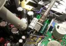
The measurements environment is to be seen in the below picture. I used a current probe set it on "Track", and minimum sensibility for lowest HF noises on the scope traces. The tension is measured using a classic probe on the same AVCC connection between the large capacity and the chip pin (pictured here).
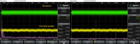
As you can see the DC tension trace it looks quite well as expected. We shall say we can ignore the HF noises on the scope traces, for this discussion. I have taken some pictures in High Resolution to simplify the traces.
Please note that the regulation for AVCC line it happen in 3 stages, where last one is a AMD7151, with the large capacity on its output.
So, where is coming from the AVCC current pulses, which it have a very precise 50Hz frequency?
I may say that I have noticed the same pattern of 50Hz in the modulated HF residual noises at the system output.
Event hough the exceptional filtering in this experiment environment for AVCC rail, even though the huge current capabilities of the decoupling cap, the chip can create these current pulses (only) on AVCC line.
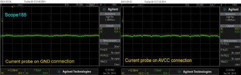
Very interesting is Vdd L/R, which do not have these pulses, but just a fine line on current. I show beside the High Resolution snapshot of AVCC line current measurement, how it looks the GND connection measured in the same configuration (marked on picture).
Supposedly, the first idea to come, is to refer to the AC main power which is going through everything. Well, I`m sceptic to this explanation. It is the same frequency (for my location), but this measurement is very far from the AC main field, as is to be found only on AVCC rail. Even more, this frequency, it modulate in a very characteristic way the HF noises at the DAC output.
To have more informations about these measurements, one should change the environment. An idea is to reproduce the measurements in a 60Hz main AC environment. Another option is to feed the DAC chip on AVCC from a battery...
I just wonder how it may looks like these current measurements on a classic powering for ES9018, if such pulses are to be seen in this one... Unfortunately I have no any measurement from the original configuration around DAC chip in this device. But if I get the opportunity, I will repeat it on a original configuration.
And to conclude for final: please remember that this power configuration I use it improve the SQ quite a lot... The audio signal on the same output used for measurements is as usual, 10Vpp.
The measurements environment is to be seen in the below picture. I used a current probe set it on "Track", and minimum sensibility for lowest HF noises on the scope traces. The tension is measured using a classic probe on the same AVCC connection between the large capacity and the chip pin (pictured here).
As you can see the DC tension trace it looks quite well as expected. We shall say we can ignore the HF noises on the scope traces, for this discussion. I have taken some pictures in High Resolution to simplify the traces.
Please note that the regulation for AVCC line it happen in 3 stages, where last one is a AMD7151, with the large capacity on its output.
So, where is coming from the AVCC current pulses, which it have a very precise 50Hz frequency?
I may say that I have noticed the same pattern of 50Hz in the modulated HF residual noises at the system output.
Event hough the exceptional filtering in this experiment environment for AVCC rail, even though the huge current capabilities of the decoupling cap, the chip can create these current pulses (only) on AVCC line.
Very interesting is Vdd L/R, which do not have these pulses, but just a fine line on current. I show beside the High Resolution snapshot of AVCC line current measurement, how it looks the GND connection measured in the same configuration (marked on picture).
Supposedly, the first idea to come, is to refer to the AC main power which is going through everything. Well, I`m sceptic to this explanation. It is the same frequency (for my location), but this measurement is very far from the AC main field, as is to be found only on AVCC rail. Even more, this frequency, it modulate in a very characteristic way the HF noises at the DAC output.
To have more informations about these measurements, one should change the environment. An idea is to reproduce the measurements in a 60Hz main AC environment. Another option is to feed the DAC chip on AVCC from a battery...
I just wonder how it may looks like these current measurements on a classic powering for ES9018, if such pulses are to be seen in this one... Unfortunately I have no any measurement from the original configuration around DAC chip in this device. But if I get the opportunity, I will repeat it on a original configuration.
And to conclude for final: please remember that this power configuration I use it improve the SQ quite a lot... The audio signal on the same output used for measurements is as usual, 10Vpp.
Attachments
Last edited:
Yes, is true, but it may happen that half of the main residual spikes/pulses it may go through... Anyway I think it is not about main AC residuals in this case. It may not be so only for AVCC, while the rest of the rails are flat (on current)... It is something about how it works the chip, but it is a strange frequency, inside the low audio spectre...
And more, how it is possible for the chip to create such current pulses (well, very small, but pulses), on a power source which is capable of an (at least) instant 10A?
BTW, there is no way to ever hear such pulses in the resulted audio signal, but why are there?
A switching device which work on this frequency, it may explain these measurements...
Last edited:
Well, some more infos about AVCC current profile... And HF noise son ES9018 outputs...
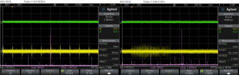
I had the opportunity to measure the same AVCC current (with the same current probe), as in previous post, but this time on a stock unmodified (configuration) device. Here the DAC chip is powered on AVCC by a LT1763 based regulator, with a 220µ at its output. The current probe is placed on one of the AVCC pins.
There is the same 50Hz profile on the current trace, but more sine or triangle wave like this time. I will explain this different pattern (compare it with the previous screenshots), by the lack of enough energy/current provided by power supplier, for the instant needs of the chip unknown process on its analogue stage.
But where it come these current pulses from? Or what it may be the chip`s analogue stage needs for quite high current on every 20ms?
Well, I took also some measurements on the same device containing ES9018, configured so as it was designed by its producer. DAC chip is clocked by a 54Mhz oscillator.
Here is more clear the pattern of this HF noise (measured on the differential/balanced post DAC output). There is quite obvious that this HF quantization noise it consist of 50Hz bursts of pulses. When these pulses are produced by the internal processes, or a switching mechanism, the chip need more energy/current on its AVCC rail. I can not know what it may be the device which is switching so on the chip`s analogue stage...
If you may go back to my previous screenshots, showing a modulated HF noise measured on similar outputs, you will observe that in my modified/improved DAC configuration, these HF noises are quite spread, or this here very clear burst of pulses (residual noises), are more confuse and mixed in between, resulting a 50Hz modulated like HF pattern.
BTW, my DAC configuration, in previous measurements, is clocked by a 108Mhz oscillator...
(BTW, was somebody who wondered about chip`s overheating when is "overclocked". The chip clocked by 54Mhz shows 40 dgC when running, while my overclocked one, it shows 41 dgC...).
I think I start to understand what is really happen, and why it sounds better my configuration...
Attachments

Last edited:
During this measurement, was the DAC playing something ? was AUTOMUTE active ?
Did you check for activity on I2C, RESET, AUTOMUTE, I2S that may correlate with this ?
Also your AVCC current looks like a filtered sawtooth, whereas the noise on the analog output looks like a series of sharper spikes. I think that if the DAC was the source, you'd see the same spikes on AVCC current as in the output.
Maybe these spikes are picked up by the analog output traces somewhere, or perhaps they come from the IV opamps power supply, or the AVCC/2 voltage reference... and then cause the DAC to draw this funny looking current.
I have not seen such spikes on ES9018 output...
Look around for a 35kHz frequency...
The DAC was not in action, while measurements. Perhaps the AUTOMUTE active... I will check this next time.
The last AVCC measurement/snapshot is taken on a stock device. There are also the small spike patterns (as in my device) in the sawtooth current trace, but they are very small. I connect the better defined current trace in my device with the very large cap on AVCC rail.
The 20ms series of the sharper spikes on the outputs noise are characteristic to the ES9018 chip. I think you should have somehow the same pattern of noise after I/V and final stages. To see this directly on the chip outputs it may be quite difficult, as their amplitude it may be very low.
This noise is obvious on the differential output lines, but strong attenuated or non existent on the balanced output. This is normal, as the unbalanced make the add function and eliminate/attenuate this noise. Also the same it happen on balanced processing, so the noise impact for the resulting audio signal it may be minimised. At least is about inaudible spectre, but some consequences for the audio signal integrity/purity it may be present...
I will try to find out more about this.
Last edited:
Member
Joined 2009
Paid Member
Coris - I'm looking at the photo of all those wires and probes in a very crowded area - I'd be starting to panic at this point ! - it's quite impressive to see your work.
Well, maybe are many other too, who do the same, but they may be quite sceptical to show or share...
It may not be reasons for panic, when you build something step by step, knowing what to do. But sometimes it happen I do wrong and then i get panic myself too... But this is not to be seen in the pictures here...😉😀
I think there is a kind of adrenaline increasing in this hobby too, as in claiming or something...
Hmmmm when I have time, I will re-measure the ES9018 output to check if I find something like that.
I'd be starting to panic at this point !
Don't look at this picture.
Attachments

Wow!!! This is really crazy... It may be a wonder to make this construction to work, but it may happen...
About the DAC outputs and this possible modulated HF noise, I have to say that I start to doubt my own findings (previous posts). I was very surprised/intrigued in the very last time to observe that everything was gone, after some improvements on the filtering stages around the DAC`s power rails (on another device than that used for tests). Unfortunately I really do not know what I have done to make this noise on outputs disappear. I have to find out about this now...
I just suspect a serious issue by design or fabrication in the device I always used for my researches/tests. It is very possible that such noises are induced by the AVCC power supply used in this device... And it mislead it me in my in own conclusions...
I may be more carefully with the published conclusions/findings...
But however I much appreciate if you will use your time to confirm or not something in this respect.
A real collaboration and each other support in researches, findings and conclusion is always much more beneficial for everybody here, than only coming out with "ego" stuffs...
Last edited:
Well, after some more investigations, I can conclude that the HF "residual"noise, which I stated so many times that it may be a normal behaviour for the ES9018 chip, it is not normal at all and it must not to be there.
There is a spectre of (modulated) HF oscillations in connection with the clock signal for DAC, which was something particular to my experimental environment (based on a modified player).
Another device which I have modified, do not present at all such noise, and its output (no signal) is a very fine line trace on scope, down on mV ranges...
You may not think at the "out of datasheet range" clock frequency, I use for my DAC, as I used the same high frequency on another device and I still not have any HF noises on the outputs, as it was to be seen in some of my previous picture here.
I is quite embarrassing that I stated so many times about such noise it may be normal... I should review my previous posts on subject and delete it. But this is unfortunately not possible.
The very big paradox in this case is that the sound quality out of that device with quite high HF noise on output is very special high... At least perceived so...
I do hope I will find some more details about this enough strange case. But first I have to find out where it come from that noise in that device I have used for my tests/experiments for so long time...
- Home
- Source & Line
- Digital Line Level
- ESS9018 - try new, try more...