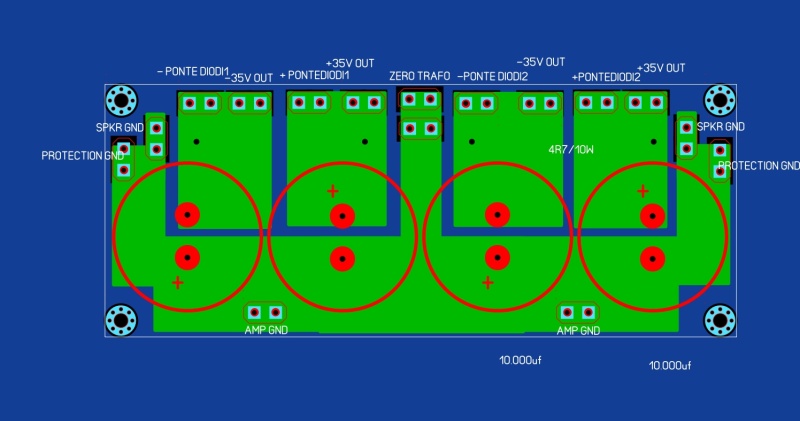
Could anybody look at this schematic and tell me if it's correctly suitable for 2 diode bridges?
Member
Joined 2009
Paid Member
I believe 0R22 can be used instead.Hey, can I use a 0.22 ohm on the emitter instead the recommended value (0.33ohm) ?
Could anybody look at this schematic and tell me if it's correctly suitable for 2 diode bridges?[/QUOTE]this pcb layout looks like you want to create something to mount the rail capacitors ? usually you'd want to include a few extra components to make a more sophisticated supply. Examples:
[url]http://www.tnt-audio.com/clinica/ssps1_e.html[/url]
[url]http://users.tpg.com.au/users/gerskine/dxamp/[/url]
[url]http://sound.westhost.com/project04.htm[/url]
Last edited:
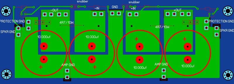
I will add snubber RC , LEDs and bypass caps.
My question was about the structure of the power supply. the last is something like the link you posted
Power Supply for Power Amplifiers
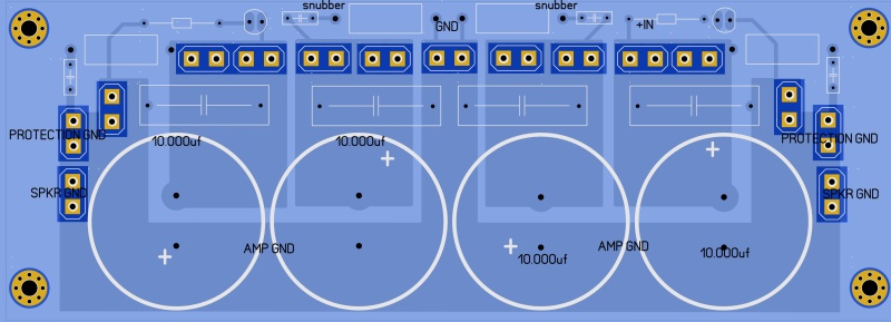
a sort of "dual mono" in which every amp will receive +V/-V from a single bridge/supply caps way; so we have the rails and the bridges connected in parallel each other; my previous layout had instead a single bridge and the caps forming +v/0 are 2x10.000 and the same the caps forming 0/-v.
so what's the best?
My question was about the structure of the power supply. the last is something like the link you posted
Power Supply for Power Amplifiers
a sort of "dual mono" in which every amp will receive +V/-V from a single bridge/supply caps way; so we have the rails and the bridges connected in parallel each other; my previous layout had instead a single bridge and the caps forming +v/0 are 2x10.000 and the same the caps forming 0/-v.
so what's the best?
I will add snubber RC , LEDs and bypass caps.
My question was about the structure of the power supply. the last is something like the link you posted
Power Supply for Power Amplifiers
a sort of "dual mono" in which every amp will receive +V/-V from a single bridge/supply caps way; so we have the rails and the bridges connected in parallel each other; my previous layout had instead a single bridge and the caps forming +v/0 are 2x10.000 and the same the caps forming 0/-v.
so what's the best?
Those were all the recommendations I gave which you implemented here, why are they removed and then put back in again?
Note, it's also very easy to make these point-to-point in free space, or point to point on perf board. Here is a very compact DX PSU based CRCLC PSU with diode bridge (buried on back end):
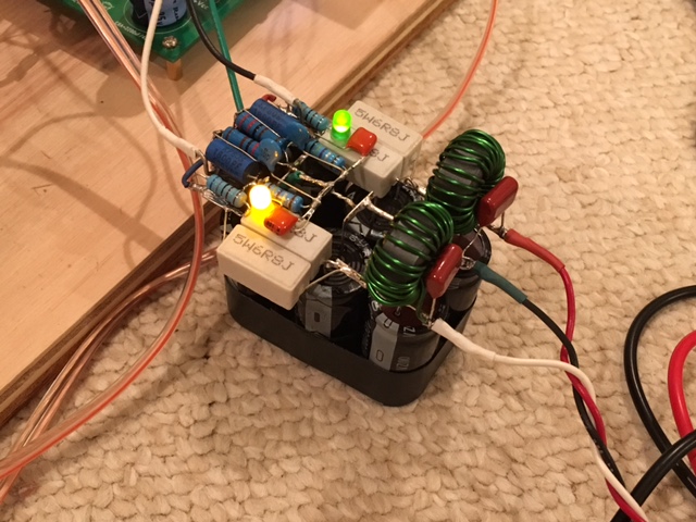
Compared to how big a Dx PSU can get when made on a relaxed perf board:
Last edited:
because the capacitors have a different orientation form the previous layout. pcb is the same but the last one is make to 2 rectifier bridge
ok, it doesn't matter
I can't find 0.33ohm for emitters.
I found 0.22 or 0.47.
which would be better?
I can't find 0.33ohm for emitters.
I found 0.22 or 0.47.
which would be better?
ok, it doesn't matter
I can't find 0.33ohm for emitters.
I found 0.22 or 0.47.
which would be better?
When I'm correct you need to set the bias recording the value you're using
for example when you use 0,22 ohm 25mV bias setting etc.
Correct me if I'm wrong
Yes the bias is calculated using omh's law. So when you use 0.22ohm the calculation is different.
But i would to know if would be a problem using 0.22 insteadof 0.33 cause mr.elliot used 0.22 in p3a but after he changed it to 0.33 cause increases bias stabity, he says.
But i would to know if would be a problem using 0.22 insteadof 0.33 cause mr.elliot used 0.22 in p3a but after he changed it to 0.33 cause increases bias stabity, he says.
Member
Joined 2009
Paid Member
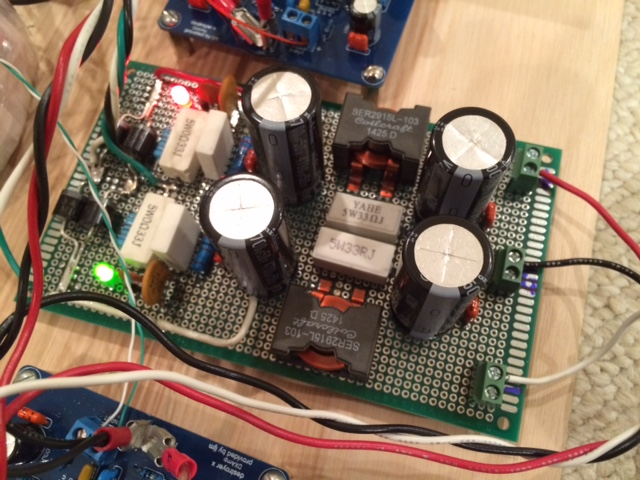
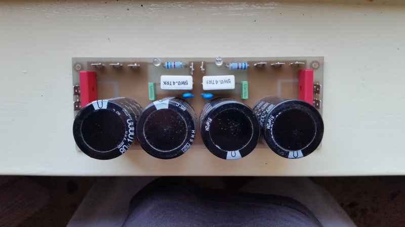
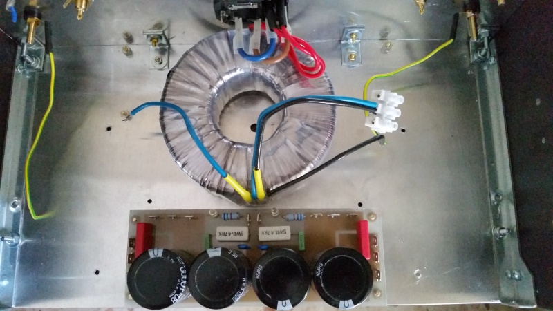
first components mounted
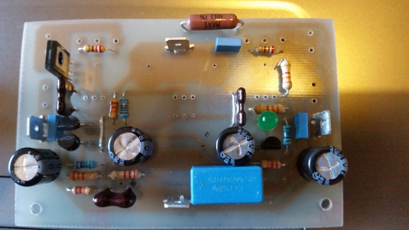
show us the underside - we want to see your soldering skills 😀
The ground lug needs more space - can you move that blue box cap to the underside ? better still, drill another hole in the copper ground bus and move the lug sideways a few mm for clearance.
Last edited:
can a good soul check this?
I have to re-make the pcb cause in the previous I missed a link in the snubber zone.
thanks a lot
I have to re-make the pcb cause in the previous I missed a link in the snubber zone.
thanks a lot
can a good soul check this?
I have to re-make the pcb cause in the previous I missed a link in the snubber zone.
thanks a lot
Where is the interconnecting R in the CRC?
There is no CRC. The schematics is this
https://www.google.it/search?q=rod+...AUICCgC&biw=360&bih=510#imgrc=QVQ5ST4QLqlppM:
https://www.google.it/search?q=rod+...AUICCgC&biw=360&bih=510#imgrc=QVQ5ST4QLqlppM:
dear cucicu,
If you post the schematics by the side of the PCB layout, it will be easier to check.
--gannaji
If you post the schematics by the side of the PCB layout, it will be easier to check.
--gannaji
this should be definitive. I hope You can check right it.
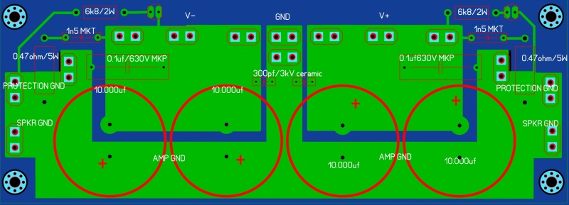
there are snubber RC, R+led, bypass caps mkp+ceramics.
If you gimme the OK, I will printi these
there are snubber RC, R+led, bypass caps mkp+ceramics.
If you gimme the OK, I will printi these
- Status
- Not open for further replies.
- Home
- Amplifiers
- Solid State
- ESP P3A Layout