Looks like about $6 more for a Crystek 549-CCHD-575-50-100 gets you another 10dB less phase noise @10Hz.
EDIT: By the way, do you use SPDIF or TOSLINK input or do you have a way to?
EDIT: By the way, do you use SPDIF or TOSLINK input or do you have a way to?
Last edited:
OK, the big Night.
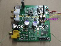
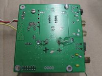
Here are the pics of the duaghterboard and DAC combined into one.
I powered it up. AVCC Feed was correct, 3.3V indicating the the 3 term regs including ams1117 was working.
Regulated AVCC was correct.
But I was still getting a positive 3 V and 9V at the output. I checked everything over six times. I changed op amps. The single op amp circuit as per ESS is simple and you could see the circuit just by looking at the board. I must have gone over that 10 times in total.
Here is what I cannot understand. With the coupling caps at the output of the ESS circuit, should there not be ZERO volts at the output?
I reused the decoupling caps originally on AVCC and repurposed them to coupling caps.
Then....
Attachments


Last edited:
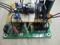
I laid out the DAC lines very carefully. The DACB lines are in Black and DAC lines are red.
Anyone see anything obvious?
Anyone see anything obvious?
Here is what I cannot understand. With the coupling caps at the output of the ESS circuit, should there not be ZERO volts at the output?
Electrolytic caps can leak a little current through the dielectric. They can also transfer some charge when you turn on the +-15volt power, and then again when you turn it off. That would occur even without any leakage current. So, there there needs to be a path to ground to discharge them. Your DVM is probably 10MegOhms input inpedance which might take awhile to discharge them but it might eventually. You could tie some 10k resistors from the outputs to ground if you want.
Also, if you are going to use opamp AVCC regulation, the AVCC caps in there now are too big. They appear to be 470uf. The ESS schematic and application note text says 47uf, or possibly 10uf could be used for certain opamps. Also, you appear to be using much longer wires for AVCC wiring that ESS recommends. My wires for that are maybe 1 cm long. Of course it is a very short distance on the back of the board to the bottom of the 47uf AVCC cap pins. Another good reason for putting everything on the bottom, that and the ground plane offers some shielding from all the RF down there in the digital circuitry. Looks like your sensitive analog circuits are right next to the RF with no shielding. Might be worth considering removing your board and the mounting spacers from the top and putting that stuff down under the bottom.
Please don't get the wrong idea from all my comments though. Very good to see you making progress.
Last edited:
Looks like about $6 more for a Crystek 549-CCHD-575-50-100 gets you another 10dB less phase noise @10Hz.
EDIT: By the way, do you use SPDIF or TOSLINK input or do you have a way to?
There's only usb and toslink.
I take the published specs with a grain of salt and wouldn't mind trying a different brand. That said an audiophile company owner has stated lately that Crystek has dramatically improved their processes since 2015 and that the random (uncurated) 575 samples he received averaged ~-108 at 10hz. The price also doubled in the last year.
Last edited:
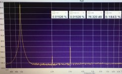
so, after relatively simple mods (separately regulated AVCC and I/V stage added ES9038Q2M Board ) THD went down from -76dB to -93dB. the SQ improvement is pretty evident - vocal "sibilance" is gone and bass is more "resolute".
in the spectrum the 3rd harmonic is bellow measurement noise floor now, however the 2nd one changed little. any suggestions what direction to dig now in order to get rid of it?
in the spectrum the 3rd harmonic is bellow measurement noise floor now, however the 2nd one changed little. any suggestions what direction to dig now in order to get rid of it?
Attachments

Last edited:
Then...part 2. In my quest to figure out what was possibly wrong I was measuring voltages directly on the ICs and the tip of my probe shorted pin 8 Vcc+ on the op amp (12V) to pin 7. That's 12V to AVCC, a tiny spark and then seconds later, I saw some smoke from the underside of the daughterboard. I think the ESS chip is fried...AVCC will not tolerate that high a voltage.
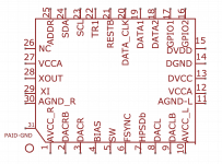
Also I was double checking the pinout of the 9038q2m. It appears that markw4 connection description on the where he connected DACB and DAC is reversed. Makes no difference in the 3 op amp output. I think.
In the single op amp solution that ESS recommends, that possibly will make a difference.
Also I was double checking the pinout of the 9038q2m. It appears that markw4 connection description on the where he connected DACB and DAC is reversed. Makes no difference in the 3 op amp output. I think.
In the single op amp solution that ESS recommends, that possibly will make a difference.
When I posted pictures of DACB and DAC it was based on looking at the Chinese boards and how they hooked up their voltage output stage. At that time we didn't have any other information about the DAC chip. Since then someone posted the pinout diagram below. It may only matter for keeping the channels in phase with each other, which seems like the most likely thing.
However, while I don't think it should probably matter which one is used for which when using the minimal IV output stage, the only way to find out for sure would be to swap the leads and try it both ways. Don't think anything could be hurt by doing that.
Sure hope the short didn't hurt the DAC chip. Sometimes smoke can be tracked to the source by smell. If something did break inside the chip it might only affect one channel which might be a way to help troubleshoot (by swapping the output stages and see if the problem moves or stays on the same side).
Sometimes I solder test points onto boards to make it easier to take measurements. A little loop of stiff wire made from the remnants of a clipped-off capacitor lead or something like that can be found and used to make a test point. Easy to hook a clip lead onto and harder to accidentally short out if thoughtfully located.
Attachments
Last edited:
@eziitis, Hard to say what to try next for the remaining 2nd harmonic. Could you post a schematic of what you did so far, maybe that could give some ideas?
Also, I would say the same to you as I did to Mike that I don't understand why put analog output stage circuitry right next to the RF part of the DAC board. While it may not be perfect locating an add-on board on the back of the DAC board and on the other side of the ground plane, it probably offers a little better shielding from close-by RF field stray coupling. However, don't necessarily see how a 2nd harmonic-only issue could be directly attributed to RF coupling, it still might cause some low-level problems and as I said, it just does't make sense to me to lay it out that way when it seems like there is a better choice easily available.
Also, I would say the same to you as I did to Mike that I don't understand why put analog output stage circuitry right next to the RF part of the DAC board. While it may not be perfect locating an add-on board on the back of the DAC board and on the other side of the ground plane, it probably offers a little better shielding from close-by RF field stray coupling. However, don't necessarily see how a 2nd harmonic-only issue could be directly attributed to RF coupling, it still might cause some low-level problems and as I said, it just does't make sense to me to lay it out that way when it seems like there is a better choice easily available.
Well Guys, I will continue to follow this thread but I need to get some other work done. In the meantime, I have ordered this DAC
ES9028 ES9028PRO DAC DSD Decoder board HIFI Audio + TCXO + remote control | eBay
Why oh why?
Already has a current mode IV, uses a 3 term 317/337 reg for the analog side....I can take those out and pretty much inject a Sulzer Power supply in there perfectly.
The AVCC appears to have its own separate power rail going all the way back to AC. If I want to put in an op amp AVCC, I could possibly just not connect the AC and then tap directly onto the decoupling caps. rather than having to dismantle the board.
The next three..er four things of significance is that it comes with a remote control, display and a slightly better crystal. One of those TXCO low jitter units that will likely get changed out in time.
For $140 delivered. Wow! with a 9028pro dac. While it all depends on implementation, I've learned enough on the SMPC board to try another.
Also I noted that this enclosure Aluminium DAC Chassis Enclosure Case for ES9038 DAC 280*62*211mm Silver/black fa | eBay will likely fit the DAC but I gotta see first. Nicely finishing metal work myself has always been a challenge.
wushuliu, I can't tell what is included with that and what isn't. There a green board, a blue board, and what looks like 1/2 of a power supply. Without more pictures and more clarity I could not see ordering something like that. The Chinese boards give you a better idea of what you actually get and what it looks like.
wushuliu, I can't tell what is included with that and what isn't. There a green board, a blue board, and what looks like 1/2 of a power supply. Without more pictures and more clarity I could not see ordering something like that. The Chinese boards give you a better idea of what you actually get and what it looks like.
This item includes the latest version PCB with ES9028PRO DAC chip and LP5907-1.2V ultralow noise regulator soldered(optional), no other component included
You get the main PCB board - and the chip soldered for extra. They explain what it comes with. The 'blue' board is their Xmos board, sold separately. I have an old version. Since they are pretty popular, they assume people know what the different boards are. The ES9038 page has a better breakdown. DIYINHK is also a member here and has been for a while. I just point them out because if going for the Pro chips, just seems their boards are much more accessible and less fussing with removing/working around unwanted components.
Last edited:
And the power supply is one of their regulators, also sold separately. I am using their TPS7whatever as the opamp power supply for my Hifime.
Well Guys, I will continue to follow this thread but I need to get some other work done. In the meantime, I have ordered this DAC
ES9028 ES9028PRO DAC DSD Decoder board HIFI Audio + TCXO + remote control | eBay
Why oh why?
Already has a current mode IV, uses a 3 term 317/337 reg for the analog side....I can take those out and pretty much inject a Sulzer Power supply in there perfectly.
The AVCC appears to have its own separate power rail going all the way back to AC. If I want to put in an op amp AVCC, I could possibly just not connect the AC and then tap directly onto the decoupling caps. rather than having to dismantle the board.
The next three..er four things of significance is that it comes with a remote control, display and a slightly better crystal. One of those TXCO low jitter units that will likely get changed out in time.
For $140 delivered. Wow! with a 9028pro dac. While it all depends on implementation, I've learned enough on the SMPC board to try another.
Also I noted that this enclosure Aluminium DAC Chassis Enclosure Case for ES9038 DAC 280*62*211mm Silver/black fa | eBay will likely fit the DAC but I gotta see first. Nicely finishing metal work myself has always been a challenge.
Hi
I have this dac for several months.
I have removed the analog power supply ...replaced by SALAS shunt reg
and replaced the Op amp by DEXA discrete Op amp
Better ....Much better


Projects:
Remove the two lt1093 (3.3v) replace by two DEXA discrete regulator (3.3v)
with a 2x6v transformer(one winding for each regulator ) ......
Why not a regulator for the crystal!!!
I'm not sure about the improvement

I will see
Serge
* Power supplies, Power Quality & AVCC per ESS
* IV Stages per ESS or Victor Circuit
* Ultra Low-Jitter Clocking
* (Optional but recommended if nothing equivalent - modded HPA $32 on ebay -105dB THD -or- Twisted Pear LME49600 HPA kit)
* Upsampling SRC
Anybody besides me planning on trying the whole works?
If all done (other than optional HPA) except the very last SRC item, and not sure about doing that one then I might have a loaner SRC board I could send out for people to try. See if you like it or not. I would be willing to pay for domestic shipping one way, you pay the return (unless you want to keep it and replace mine). International shipping, we would have to see - don't know.
The reason I would like to make the offer is because I think people generally can understand about power supplies and clocks, and getting THD down with an IV output, and those things are probably within most people's budgets to get to, especially as others do and post their results. On the other hand, an SRC is less commonly understood as a component of a good DAC and it is an expensive thing to try without knowing how much it might help and without having other people posting their results with their own different degrees of modding. For the above reasons, it may be too much to expect people to a take a chance, or to buy into one person's recommendation (mine 🙂 ) without anything more than that. The reason I want to limit to people who already did everything else is because they are the most likely to be able to hear what the end result of all the modding can sound like in the context of an SRC being the last touch. Trying it before then might not give a good idea of just how good the end result can be.
Last edited:
You get the main PCB board - and the chip soldered for extra. They explain what it comes with. The 'blue' board is their Xmos board, sold separately. I have an old version. Since they are pretty popular, they assume people know what the different boards are.
I looked at the link you posted, but I still don't know what know if it has a microcontroller on the board, jumpers, and or how one might select the reconstruction filters or desired input? What about volume control? Maybe the only way would be to buy the 'optional' XMOS board? If the DAC can't be operated without an optional board it starts to sound less optional. 😕
Since we don't have any specific recommendations people can use relative to predictably finding a good power supply, I am hoping to try a few options early next week and report back with whatever the findings.
However, in that area something rather interesting just happened. I decided to play around with a small brick +-15v @1A switcher I think I got from maybe Mouser at some point. Tried it before but it was way too noisy, in the EMI/RFI sense. Anyway, took a small Hammond electronics enclosure box and lined the inside with copper foil, bolted the output ground to the case, brought out the +-15v through two RF feedthroughs (one for each output), and screwed the lid down tight. Still didn't work, too RF much hash everywhere. So, put a ferrite torroid around the AC line inside, put a few torroids over the output and ground leads just outside the feed-throughs, and then fully wrapped the outside of the metal box in yet another layer of copper foil. Viola! Not hearing noise on the shortwave radio tracing the leads with the wire antenna and searching around the outside box surfaces. Unfortunately, since it is a 1A. switching power supply I need to run it at least at 10% load to maintain regulation. That is a bit more than I have test loads for at least for more then an a very short time. So, it may be a 2 or 3 days or so before I will know much more.
At that time also have some more linear power supply options to look at, but at least now I feel like there might be some hope to find a switcher solution that could work. If so, that would potentially reduce case size needed and also cost for a finished DAC project. Just need to make sure I leave room for the SRC board, wouldn't want to have to leave that out. 🙂
Last edited:
I found this power supply on the bay using 2 LT1083CP chips for a low noise +/-15V PSU. Add a $30 toroidal transformer. You get a pretty good quality linear PSU for $50.Since we don't have any specific recommendations people can use relative to predictably finding a good power supply, I am hoping to try a few options early next week and report back with whatever the findings.
The LT1083 is not as low noise as the LT3045/TPS7A3301 pair, but is far superior to the LM317/337 pair. Hope you can consider this. I have the parts enroute to me now.
An externally hosted image should be here but it was not working when we last tested it.
Last edited:
- Home
- Source & Line
- Digital Line Level
- ES9038Q2M Board