Okay, in that case what I would probably want to try would be to use three dc-dc converters, one for +5, one for +15, and one for -15. I would connect the ground of the 5v supply to the dac board ground plane near the dac chip. I would connect the +15v ground near the opamps, and I would also connect the -15 ground near the opamps. I would not connect the grounds together at any other place (i.e. not on the power supply board).
I say that based on experimental results with my previous dacs. Also, even if that doesn't turn out to ideal you can always move each ground around to find the best spot for it.
Now, a word of caution: What I suggest might not be a good idea if there is high line noise leakage through the dc-dc converters. In that case some noise ground loops could be created by connected the grounds together only at the dac board. A better solution in that case might be to tie all the grounds together at power supply, or to make all the supplies share a single ground plane on the power supply board.
In my case I am using R-core transformers with separate windings for each supply, so line noise leakage is very low. Also, I didn't use any SMPS. Using medical grade SMPS modules may help reduce leakage currents, but that might increase cost some.
IMHO ultimately designs on paper have to be evaluated and revised based on prototype testing, at least if the goal is to have a commercial quality end result.
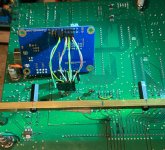
Thought I might post a pic of one way to connect a USB board to a DAC board with pretty short wires that are twisted into pairs. Each pair consists of an I2S signal and a dedicated ground. The wires are lightly twisted and separated from each other to help minimize stray coupling between pairs. Also the USB board ground plane is facing towards the end of the dac board where the dac chip is located; the USB board is also on the solder side of the dac board. Another way I might have done would be with the USB board ground plane facing the DAC board ground plane (i.e. with the USB rotated 90 degrees from the position shown in the pic). Experiments showed that least amount of audible stray coupling effects between the boards occured with the above configurations. Of course depending on local particulars YMMV.
Attachments
Last edited:
That is fine Mark, do you else have anything new?
Have you read about Topping how they coupled 8 channels together for improved sound quality in
ES9038 pro dac?
Do you think it works or just another marketing trick?
Have you read about Topping how they coupled 8 channels together for improved sound quality in
ES9038 pro dac?
Do you think it works or just another marketing trick?
Nothing new to report on dacs. Still been helping a friend with some discrete analog audio stuff for the past few months. Probably I will return to dacs at some point, but with the loss of AKM it may take awhile before something new comes up that is interesting enough to pursue.
Regarding Topping, IMHO they needed to do something when they lost access to AK4499. ES9038PRO may be the next best thing. However probably still sounds more or less like ESS dac chips tend to sound. Haven't heard the new Topping myself, so no personal opinion on it.
Regarding Topping, IMHO they needed to do something when they lost access to AK4499. ES9038PRO may be the next best thing. However probably still sounds more or less like ESS dac chips tend to sound. Haven't heard the new Topping myself, so no personal opinion on it.
Last edited:
My configuration.
R-core. 15-0-15, 9-0, 9-0
Lm317/lm337 to opamp
Lm317 for another parts
Lm7805 for digital part
3 pcs Ltc6655 for avcc, clock, dvdd, vcca.
Change clock on Crystek cchd575
Transport amanero
R-core. 15-0-15, 9-0, 9-0
Lm317/lm337 to opamp
Lm317 for another parts
Lm7805 for digital part
3 pcs Ltc6655 for avcc, clock, dvdd, vcca.
Change clock on Crystek cchd575
Transport amanero
It usually isn't so much that bass disappears as it is that too much brightness is added to everything, including to low bass instruments. Getting rid of the added brightness often seen with ESS dacs may not be trivial. That said, sometimes bass can be weak too, but IME its not usually the main problem with dacs.
Regarding LTC6655, it is a voltage reference only, not a voltage regulator. LTC6655 has been suggested as a reference voltage source for opamp buffers to drive AVCC_L and AVCC_R. There is no reason to use LTC6655 for anything else.
For DVCC, VCCA, and Clock, I have said that I used three dedicated LT1763 regulators, each with an extra load resistor to ground (to bias the regulator at a moderate output current). For the clock, I use 805 size SMD film bypass caps. I don't use ferrites for clock power or anything else; haven't needed to. Wouldn't use them myself unless they are proven to be needed in a given situation. The LT1763 are all powered from a shared clean +5v rail.
Keep all the final stage regulators physically close to their loads and mounted on the same ground plane as the dac chip.
All the above stuff is the same stuff I have been repeating for a long time. It works.
Also, for ESS dacs it is important to run DPLL_Bandwidth at the lowest stable value (as ESS recommends). What low value are you able to set it to?
The output stage is yet another problem to get right. First just get the I/V part right. Maybe listen to that part first before going on to differential summing design. Does I/V output have bass and sound okay?
Last edited:
The LTC6655 can only source 5mA. Have you buffered them with something a little more beefy?
I'm not understanding you...
It sounds dull, and there is weak bass too?
I don't know if opamp buffers are the best way to drive DVCC, VCCA, and Clock power. Never tried it. Where are the opamps located? Do you have high res pics you can post? That would probably help a lot...
I don't know if opamp buffers are the best way to drive DVCC, VCCA, and Clock power. Never tried it. Where are the opamps located? Do you have high res pics you can post? That would probably help a lot...
Last edited:
Crystek should not be a problem unless maybe the power supply for it is wrong. How is it powered? Do you have a schematic and or pics for it? For dacs, layout matters; it can matter a lot, that's why we need to see clear pictures of the layout and wiring.
Measure the frequency response and see what and how much it changed before and after.There is no brightness. On the contrary, it sounds dull
- Home
- Source & Line
- Digital Line Level
- ES9038Q2M Board