I read that, but I still don't know how an opamp with VEE connected to ground, VCC connected to well regulated +12V, configured in gain = +1 configuration, fed with well regulated and filtered +3.3V at the noninverting input is in principle different from any other voltage regulator.
It has a stable/low noise voltage reference, PSRR that matters is that on the VCC pin and output impedance is defined by it's open loop gain vs frequency.
I'd appreciate it if you took the time to point out where exactly I'm wrong with my assumptions and not tell me to read up on basics. What basics?? Education works in three ways:
1. explain the necessary facts and principles at hand
2. tell where to find further information
3. practice
It would be your job now to provide 1. and 2. - assuming you want to participate and be the teacher. If not - well, you're just outputting unuseable information for the good of nobody. Information wants to be free.
aka Long live piracy.Information wants to be free.
I think you will find it neither knows nor cares about freedom.
This is a DIY forum and copyright infringement aka piracy can never be conducted by a private person. At least that's the law here in Europe.
And seriously, we're talking about information here that's freely available in datasheets, willingly put out into the public by IC manufacturers, so what the heck are you trying to say?
Your last sentence isn't even a correct english sentence. No wonder I'm having trouble to understand it.
And seriously, we're talking about information here that's freely available in datasheets, willingly put out into the public by IC manufacturers, so what the heck are you trying to say?
Your last sentence isn't even a correct english sentence. No wonder I'm having trouble to understand it.
"...last sentence isn't even a correct english sentence."
The sentence reads okay to me. Its sort of a metaphorical/poetic following to the prior sentence though.
On the topic of information wanting to be free, it depends a lot on who pays the cost of developing useful information. Its not free to discover some information; it used to be more free because the government funded more of research instead of private industry doing it. Also, the patent system was created in principle to encourage voluntary sharing of information.
Regarding this diy forum, I have dropped plenty of hints about how to design a very good dac. Have I said everything I have learned about it? No, but maybe someday, and even now sometimes I help specific people more by PM. Did it cost me a lot of time and effort to figure what works and what doesn't? Yes. Take what you get for free as a starting point then do some of the remaining work for yourself. See how you feel about giving it away after that. If you still want to share, we await your contributions to the dac sub-forum with interest.
Last edited:
...Which would be good, but only if it would be required; a competent engineer would attempt to figure this out, before designing in the op amp buffer. An incompetent engineer will say "an op amp buffer is good because it sounds better".
Nonsense. The way I doo things saved your *** once:
ADCs and DACs for audio instrumentation applications Post #582.
ADCs and DACs for audio instrumentation applications Post #592.
Did you study the problem like a PhD and publish a paper on it? No.
Anyone can read the rest of the thread and find no experimental evidence of why the fix works from you. Only some speculation.
What actually happened is you found a fix and once you found it then you moved on to the next problem. Same thing I do. When I find something that fixes a problem for me, I don't study it to death and publish on it. I move on to the next problem.
And just like you sometimes I conjecture about why the fix might have worked, and like you I do it with no publishable confirming evidence.
ADCs and DACs for audio instrumentation applications Post #624
However, in your case of your thoughts you missed the fact that sometimes lowering Vcm is not the fix; so, that it cause a dc bias current to flow can't be the whole explanation.
Please see the follwing for links to evidence you neglect to explain, and that tend to contradict some of your conjecturing:
ADCs and DACs for audio instrumentation applications
Last edited:
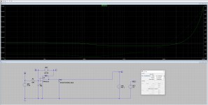
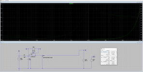
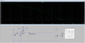
As promised here are the Zout and phase margin graphs from our simulations for the OPA1611 AVCC supply.
Is it possible to provide simulation * .asc
Thanks.
...here are the Zout and phase margin graphs from our simulations for the OPA1611 AVCC supply.
No resistor to represent the AVCC load presented by the dac chip?
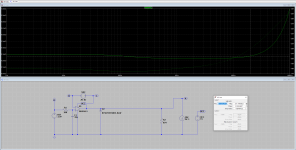
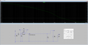
Its small signal output impedance could be a little bit operating point dependent. Its that when trying to be accurate at or below -120dB levels, tiny things can matter. Don't know how good the opamp model is though. Maybe someone could hear smaller deviations than can be accurately modeled. At least, some professional audio designers I know don't model at all because they don't believe the models are accurate enough for what they are trying to do.
As an aside, I am helping a friend do some work on the beginnings of a commercial prototype specialized preamp (and doing it for free). The number of listening tests involved in optimizing the sound is a lot, a couple hours of it every day for weeks. Its a complicated optimization problem with the goal being to satisfy human some or most of human listeners. Its a process I didn't expect to be so long and tedious. IMHO the number of subtle variations on SQ is pretty interesting.
As an aside, I am helping a friend do some work on the beginnings of a commercial prototype specialized preamp (and doing it for free). The number of listening tests involved in optimizing the sound is a lot, a couple hours of it every day for weeks. Its a complicated optimization problem with the goal being to satisfy human some or most of human listeners. Its a process I didn't expect to be so long and tedious. IMHO the number of subtle variations on SQ is pretty interesting.
Last edited:
I have a question about return current. And proper ground to ground connection.
I have 2 seperate board. One is dedicated for dac. The other one is power supply.
DAC board have clean ground.
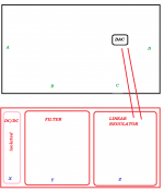
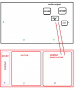
Power supply board has isolated dc/dc converter then filter section and finally linear regulator.
Which location (A,B,C,D TO X,Y,Z) or any other is best places for ground connection from power supply to dac board?
I have 2 seperate board. One is dedicated for dac. The other one is power supply.
DAC board have clean ground.
Power supply board has isolated dc/dc converter then filter section and finally linear regulator.
Which location (A,B,C,D TO X,Y,Z) or any other is best places for ground connection from power supply to dac board?
Attachments
Last edited:
Is the power supply board sharing one ground for the dac chip and the analog output stage? If so, not ideal from my perspective.
Hello Mark;
The power supply consist linear regulators for dvcc, avcc, osc, opamp, vcca.
I can make multiple ground connections between two board just need to know where is the best location?
The power supply consist linear regulators for dvcc, avcc, osc, opamp, vcca.
I can make multiple ground connections between two board just need to know where is the best location?
Attachments
Last edited:
Do you have a schematic of the power supply board? Does your power transformer have separate secondary windings, or center-tapped?
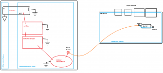
Well there is no transformer its main power source is 5V isolated SMPS
I wonder "return curents" are returning to linear regulator ground connections or the to the isolated dc/dc power source ground?
I wonder "return curents" are returning to linear regulator ground connections or the to the isolated dc/dc power source ground?
Attachments
Last edited:
So, is the plan to run everything from one +5v rail? How will +3.3v be produced for devices that need it? What is the plan for cleaning up the switching noise from SMPS?
It would sure help to see a schematic, even a pencil sketch of one showing the overall power supply design. A dotted line or some connectors could be used to show which components are on the dac board, and which are on the power supply board.
It would sure help to see a schematic, even a pencil sketch of one showing the overall power supply design. A dotted line or some connectors could be used to show which components are on the dac board, and which are on the power supply board.
My plan is to use two dc/dc converter one with 5v output one is ±15v output. To clean up noise, LC filter + cap multiplier right after isolation then use a linear regulator 3.3v and 12v output. Then i will connect each output to the DAC inputs with cables.
The dac pcb will have isolated I2C and I2S inputs. So dac pcb ground will be clean.
The dac pcb will have isolated I2C and I2S inputs. So dac pcb ground will be clean.
Attachments
Last edited:
- Home
- Source & Line
- Digital Line Level
- ES9038Q2M Board