Hope today's picture activity is not causing too many notification emails going out to everyone. Think I am about done with pics for today, but would like to show one more that I think should hopefully be enough for now for those people asking for more details as to how to go about building something like the through hole component output stage.
Of course, you know I will ask a question at some point. So, may I ask if anyone else has already started in on this project by getting some parts together, or maybe even by test fitting a little piece of perfboard to the dac board, or whatever it may be?
Also, should probably mention that I heard from Allo regarding Katana 1.2 which was to the effect they that are still testing the new filter setup and will let me know when they have more to say. That sure is a lot more vague than previous information that 1.2 was imminently ready to ship out to reviewers, but today's update is at least honest in that they don't say they know exactly what the shipping time frame is going to be. Looks like the message was more in the, "hang in there guy, we haven't forgotten you," type of reassurance offering. That's okay with me, actually, because I want to see Katana be the best it can be.
However, with regard to making Katana and also our little modded dacs better, occurs to me we may hit a limit. I say that because I have been thinking some more about the little clues dropped by Benchmark about their dac technology. (I don't give up easily.) And, I think I will probably have something to say pretty soon about my more recent musings as to how I am thinking they get that really good sound quality. If that might in some way be considered good news, the corresponding bad news would be that to continue making progress with our DIY experiments for ever better dac sound quality we will probably have to make the move at some point to working with PRO chips and leave Q2M behind. Oh, well. Way it is. Just have to deal with it I guess.
Attachments

Last edited:
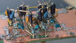
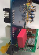
A little more progress on the through hole component output stage board. I am finding that it is a bit tight in there because I prefer to keep leads fairly short, at least where possible.
That being said, for others interested in building one of the output stages it might be worth considering moving the sockets a hole or two farther apart to ease construction access. Latest pic below.
That being said, for others interested in building one of the output stages it might be worth considering moving the sockets a hole or two farther apart to ease construction access. Latest pic below.
Attachments

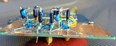
A couple of pictures below.
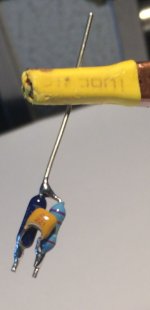
First is a picture of sub-assembly for attachment to output and inverting input of differential summing stage, one needed for each channel.
Second picture is of completed components and sockets wiring. (6.8nf output filter caps are tacked on lightly until I see how I like them.) I/O wiring on the bottom of the board, and power wiring on the top, both remain to be finished up.
Will probably add some 1,000 uf power filter caps somewhere, maybe on the dac board or maybe on the output stage board. I also usually like to put some reverse protection diodes where power comes into a board like this if it is not equipped with a polarized power connector.
Looks like it is getting about time to start laying out an AVCC power supply somehow or other. Want to have ground plane for it too. I guess I have some ideas about how I might do it, but they aren't quite solidified yet. Anyone else been thinking about how to do AVCC? Serge, have you by chance made any progress on figuring out what to do for LTC6655 output filter cap? I only have some physically big ones here. May just have to go with that.
Attachments
Last edited:
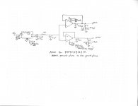
Given the number of downloads of the recent rather poor quality AVCC schematic it appears there was more demand for one than I had realized. I would therefore like to offer a slightly improved version in case it would be helpful for working on a through hole component AVCC board.
EDIT: Error got through on drawing during a revision. Opamp(s) are intended to run on +-15v with decoupling caps on both rails, or alternately, +15v and ground could be used, with decoupling just for +15v. Don't know if it makes any difference which power scheme is used in terms of SQ, but I wouldn't expect any difference.
EDIT: Error got through on drawing during a revision. Opamp(s) are intended to run on +-15v with decoupling caps on both rails, or alternately, +15v and ground could be used, with decoupling just for +15v. Don't know if it makes any difference which power scheme is used in terms of SQ, but I wouldn't expect any difference.
Attachments
Last edited:
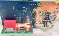
Since nobody has anything to say today, not sure why, I guess I will try to keep moving along by getting something going for AVCC. I am thinking of putting a little board on it's side under the dac board so that the opamp outputs can be pretty close to the AVCC caps leads on the bottom side of the dac board. The mock up is pretty crude in that regard at the moment, but it is just to illustrate the basic concept. I would probably put the opamp socket on the other side of the board and arrange the output pins for a pretty direct path to where AVCC power needs to go into the dac chip.
In order to mount a board there, I might need to move the audio output RCA jacks down to the output stage board, not sure. Might be a better place for them anyway.
Probably could fit the Vref dividers on the little AVCC board too. I was thinking of only having the ground plane make contact around the middle area of the dac board where the old output stage was. I laid a piece of copper foil roughly in that area to illustrate.
Closer to the far end of the dac board down where the digital stuff is would be an area where I would probably not connect the ground planes together. That would approximately be under where the far end of the big film cap is, for example.
Attachments
Hi Mark,
Thank you for the pictures
I'm not at home for 10 days.
I will order parts on monday and start the mod when coming back home next sunday.
Will you provide some synthetic pdf like Serge did?
Beginners could learn from a step by step tutorial to help them understand each phase so they can make progress.
Hi terry22,
Since you ask, I could try something like a pdf. However, I did post the pictures here in the same order they would appear in a pdf. I also tried to take them often enough and from a good angle enough so as to make them useful for a how-to pdf. The pictures are also intended to be used with the layout drawing so one could compare the layout drawing with the pictures to better understand how the layout drawing is being used to guide construction.
What I don't know and cant know unless people tell me is how much exact detail I should go into. If too detailed, it would make a pdf harder to use, and if not enough detail then more or less the same problem.
I could just copy the pictures in the same order they appear here into a pdf, along with the schematic and layout drawing, then say "add the next capacitors and resistors as shown in the next picture" over and over again for some of it. If that's what people want, and it's about what Serge seems to be doing, then sure, I could do that. My only question is, is that in fact what people want and need or should I do something different from that?
Interestingly, this thread seems to be dying. Number of views per day is plummeting. Don't know why exactly, the numbers never fully made sense anyway.
Well, we will get through this construction phase in a few more days, eventually Katana dac will be back around, and some other interesting things may be going on. We will see if there is any correlation between content and views or not.
Present blip could be entirely unrelated to this how-to construction focus going on at the moment. Hard to say, but curious to keep an eye on.
Also, I do think people interested in prototyping could learn something here (professionals excepted of course). I still see people in other threads trying to evaluate the sound of dacs with wires running all over the place and up in the air. Can't see expecting any kind of accuracy that way. I struggle over how to make these layouts electronically high quality for good performance. Don't know exactly how well things will turn out with the present project, but we will see.
Last edited:
Markw4,
the thing why this thread seems to die is that with your building of through hole design you are adressing to absolute beginners that are not able to transform a schema into a physical design. I appreciate your idealsm and your big efforts you spend into it, but dont be surprised that people with higher knowledge are not feeling involved in discussions about such basics when the discussion here was already much further developed..at least it seems to be this the reason for decreasing interest to me. Dont know why so view feedback from the ones you wanted to adress to with this simple design.
To me it would be much more interesting to see e.g. the new board I pointed out here a view days ago to be modified and I cannot see the benefit of a through-hole design compared to your (and mine) smd solution. It is really not so much more difficult in smd and you can also use the already existing onboard opamp what makes the new i/v board less complex. One thing that really interests me about the through hole board is if the new filter has better SQ and if opamps still run that hot. And I like the photos, but for me as said above small is more beautiful..;-)
Hi freezebox,
Sure, I see what you are saying. By the way, I did order a new board with a different layout, but it was rejected entry by customs. Don't know why, maybe part of the trade wars. They used to be pretty lax about not requiring a customs declaration on small packages. Don't know if that was the problem or not. Anyway, I ordered another one, but work on that is delayed.
Agree with you about interest in the new filter, and to see how it may affect SQ.
Also, at some point I would like to bring the discussion back around to Spartan 6 and DSD. Might have to be multichannel DSD though, not done looking into that aspect. Do have a slow 50MHz Spartan 6 board on its way from China to play around with. Maybe fast enough to try some limited things, don't know.
Being old and retired, I am not as fast a picking up new things, getting actual work done, and or having stamina to work long hours. But, still keep moving along, just slower is the main thing.
I do think it is very interesting that so far my modded dac, which was built with very little in the way of test equipment and no simulation has turned out when compared with other dacs as was fairly recently done. Don't know how the next iteration will go, but, should be interesting to see.
Also, I keep wondering about all the focus on NOS dacs that goes on around here. I haven't built one, and I don't think any of those guys have built one of our dacs here, at least not a fully modded one. I would like to hope that we can learn how to make modern dac building a more interesting option for people who want good sound quality and think Sabre dacs have to be clinical and fatiguing. They don't have to be like that, IMHO.
Also, I am interested in seeing if we can sort of marry the best of Sabre dac and opamp technology with transformer outputs and other things people may think they like, or just want to have. I believe we can keep the opamp sound inaudible or nearly so simply by avoiding opamp output stage cross-over distortion by way of biasing them to operate class A. That is easy enough to do in the I/V stages, but not in the differential output stage. What I am thinking of trying is bridging a transformer differentially across the I/V stage outputs. I should by able to try that easily enough with the through hole output stage board. Easy to grab onto those signals with it. Still may have to figure out how much remaining RF gets through and what to do about that.
Another thing I am thinking of trying is turning down Clock_Gear in the dac chip control registers. That would operate most of the dac at a lower internal clock rate without changing the external physical clock. While that would limit the highest sample rate we could play back, it might very well substantially reduce RF leakage. If we get the maximum frequency RF down to within where the opamps behave reasonably like opamps we might some some reduction in distortion on that account. The ability to do that in the registers is ostensibly to save power, but it would at least be something perhaps worth trying to see if any audible results.
Lastly, I would like to say that I don't know if I can walk and chew gum at the same time, but I think we should be able to talk about multiple topics at once. The building thing will be over pretty soon anyway. I am slower at it than I used to be, but we're getting there. And I really do want to make dac modding accessible to people who want it and could probably do it with a little bit of hand holding. Everybody here who is very experienced wasn't always that way, right? Way back when, they might have appreciated some help with things they didn't know how to do. I know I would have. I can remember wanting so badly to understand how to design, but just not having it click. In more recent experience, I have seen some recent graduate engineers, even some with advanced degrees, who need some help at first. So, I hope people who have gotten past a lot of that don't get too snooty about it in others.
Last edited:
Given the number of downloads of the recent rather poor quality AVCC schematic it appears there was more demand for one than I had realized. I would therefore like to offer a slightly improved version in case it would be helpful for working on a through hole component AVCC board.
EDIT: Error got through on drawing during a revision. Opamp(s) are intended to run on +-15v with decoupling caps on both rails, or alternately, +15v and ground could be used, with decoupling just for +15v. Don't know if it makes any difference which power scheme is used in terms of SQ, but I wouldn't expect any difference.
With your AVCC ref voltage, you can use more aggressive LF filtering, say
100uF after the 10k R (instead of 10uF) and bypass 10k with a small
schottky pull up diode. Just a trick I've used on quite a few things where
I want very low LF noise.
T
@Markw4
True....! Seems to be my default state.... at least I know enough to be mains safe, to test and ask and check more than twice before switching on....(patience is a virtue,... and it helps retain the magic blue smoke)
Mark, can you take a couple of pix without the flash and with some side-lighting ?
..... your macro is good but the depth of field not so much.
..probably limitations of P&S camera...?
and the flash flattens everything at the board level so it is very hard to tell what goes where...
thanks,
Bob.
Everybody here who is very experienced wasn't always that way, right? Way back when, they might have appreciated some help with things they didn't know how to do. I know I would have. I can remember wanting so badly to understand how to design, but just not having it click.
True....! Seems to be my default state.... at least I know enough to be mains safe, to test and ask and check more than twice before switching on....(patience is a virtue,... and it helps retain the magic blue smoke)
Mark, can you take a couple of pix without the flash and with some side-lighting ?
..... your macro is good but the depth of field not so much.
..probably limitations of P&S camera...?
and the flash flattens everything at the board level so it is very hard to tell what goes where...
thanks,
Bob.
Hi Bob,
Don't you mean more like PoS camera? 😱
Actually, there are two cameras here, the one in my phone and the other a roughly 20-year old Kodak DX7440 digital. Mostly I use the phone camera, always with flash disabled and either side-lighting or natural light. Problem is that copper foil produces terrible glare with most lighting. (Same glare issue with the Kodak, so no flash ever used with it either.)
The Kodak camera at least does allow manual exposure settings except for focus (auto focus only), but to get good depth of field requires smaller aperture settings and thus longer exposure times. Problem there is I cannot easily hold it steady enough for long exposures without unacceptable blurring. The other issue with depth of field is that because of not many megapixels, I need to get close to the circuit board to get good spacial resolution with sufficiently fine-grained details. Closer distance also tends to make good depth of field more difficult because of different relative distances of different objects in the field with respect to the lens. If both lots-of-megapixels and the camera a long-ish distance away, then since all objects in the field are about the same relative distance from the camera, good depth of field and sufficient spacial resolution could both be possible at the same time.
At times I have taped the camera to a mic stand to help stabilize it for longer exposure times, but then removing it from the mic stand is tedious every time I want to hook it up to a computer to download the pictures. Also, operating the button to take a picture still shakes the whole mic stand some.
The reason for not having a more proper camera and associated accessories around is because I am someone who essentially never whiles away the time looking at old photos, something I found out about myself long ago. If I have seen a photo once why do it again, I already know what it looks like.
However, looking pictures of components can be different. In that case we may care about a lot of little details of positioning and so forth. Hard to justify a fancy camera for those relatively rare occasions.
Anyway, not sure what to do. I probably need a better camera with a reasonable number of megapixels, an adjustable support arm for positioning it, and a remote trigger button so as not to shake the thing when taking an exposure.
Guess maybe I could try taking outside in the sunlight tomorrow and see what kind of picture I can get there. Maybe better in terms of a more diffused light source.
Last edited:
Problem is that copper foil produces terrible glare with most lighting.
A makeshift diffuser between the light source and the subject would help... a sheet of tissue, white cloth, or even some waxed luncheon wrap...
one of the $2 phone mounts for cars can be adapted to hold the phone still and android phones can be triggered by voice command...no button needed...🙂
Voice Camera Free - Apps on Google Play
How to Make Any App Work With Voice Commands on Android
or this...
https://www.dx.com/p/wireless-bluet...phone-android-device-with-bt-4-0-black-425605
https://www.dx.com/p/small-desktop-...r-samsung-htc-xiaomi-more-silver-black-260077
Thank you for the photography tips. I will look into them.
In the meantime, I don't have any holders or remote exposure buttons yet. May I ask if the existing pics and layout drawing are usable or not as they are? I thought they were insofar as looking at a jumble of wires and components can be easy or hard to visualize in 3-dimensions when only 2-dimensional clues are given.
In other words, if I just look at the output stage board in-person it is not that easy to see what is connected to what except by turning it in my hands so my System 1 brain processes can pick out what is in motion relative to what, and pick up more 3D clues from that. Or, sometimes looking at it with a little flashlight helps. Not sure any photography is going to make mental visualization a whole lot easier, if that is the problem you are wanting to see improved.
But, like I say, I think it works with the layout drawing in one hand and with the pictures blown up to full size by clicking on the white X in the lower left corner, it is possible to work through it. No?
@Terry Demol,
Thank you for the trick. See what you mean. Don't know if I need it for this, but I will keep it in mind. Obviously, the type of diode selected would depend in part on the nature of noise expected to need filtering out. If it can exceed enough volts to bias on a diode, or partially bias one on, that could be a consideration in whether or not to use the trick, or maybe to select a diode with a higher forward drop knowing turn-on time filter charging will take longer.
Also, want to thank you for taking the time to contribute and to let yourself be known around here. May I ask if you just happened to be passing through, or if you have any ongoing interest in our dac modding efforts?
Last edited:
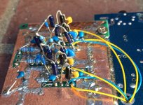
Tried taking a several more pics in outdoor diffused light. A couple might be useful, although not so sure about one of them. Angle may make a big difference, but there are not many good angles possible. You can see what you think.
EDIT: It may help to be aware that there are 4 distinct nodes tied together up in the air. Some of them stretch over longer distances from the more outside I/V opamps, and they have components attached at various places. The nodes for the more centered I/V opamps tend to come together at one solder blob each. I could try marking the 4 aerial nodes in different colors if that might help to distinguish them. If you want me to give it a try, tell me which picture would be best to do that with.
EDIT: It may help to be aware that there are 4 distinct nodes tied together up in the air. Some of them stretch over longer distances from the more outside I/V opamps, and they have components attached at various places. The nodes for the more centered I/V opamps tend to come together at one solder blob each. I could try marking the 4 aerial nodes in different colors if that might help to distinguish them. If you want me to give it a try, tell me which picture would be best to do that with.
Attachments
Last edited:

Mike or Mark?
If Mark, the opamp will be in a socket, but presumably LME49720 would be the default. Thank you for chipping in with some help, whoever it is directed at. 🙂
If you are referring to Mike's plans to use LME49600, that is only necessary for PRO chips, or one possible way to do it for PRO chips. A rather expensive way, as it happens.
A third possibility is that you are starting on a layout drawing as we discussed?
Last edited:
Mike or Mark?
I wanted you, Mark. So I can go ahead.
Thanx for your fast replay.
- Home
- Source & Line
- Digital Line Level
- ES9038Q2M Board