Well this is the situation. I have ordered some LME49600. The footprint is the same as the LT1963. Upon removing the LT1963, the LME49600 will take its place. Placed on top of that will be an LME49710 with the pins reaching out so that the circuitry is device to device. The Solder tab on the LME49600 is Vee which will be attached to the grounding pad on the main board which is viaed to the inside ground plane of the DAC board. I will be using an LTC6655 which I received from maleetronic.com a couple weeks back. So essentially the AVCC supply will mostly be device to device with some point to point directly to the ground plane for low impedance. The soldered tab to the ground plane will provide lots of heat dissipation for the intended application with no fear of overheating and device shutdown.
Paper work first
Sorry guys, but I'm behind schedule with the diagram. This week was quite busy in the evening as well. I hope to work on it this weekend.
Hans-Peter
Sorry guys, but I'm behind schedule with the diagram. This week was quite busy in the evening as well. I hope to work on it this weekend.
Hans-Peter
http://www.ti.com/lit/ds/symlink/lme49860.pdf
http://www.ti.com/lit/ds/symlink/lme49720.pdf
Is the LM49860 just a higher voltage version of the LME49720. Compare and decide. The characteristics are certainly different when you look closely.
http://www.ti.com/lit/ds/symlink/lme49720.pdf
Is the LM49860 just a higher voltage version of the LME49720. Compare and decide. The characteristics are certainly different when you look closely.
Sorry guys, but I'm behind schedule with the diagram. This week was quite busy in the evening as well. I hope to work on it this weekend.
Hans-Peter
Hi Hans-Peter,
Thank you so much for replying. Never know what is going out there in the rest of the world unless I hear from folks.
I know you agreed to commit an hour of time to giving it a try. If you can find the time at your convenience, I would still encourage it.
----------------------------------
For our other beginner's out there, maybe we can go through trying to work on a layout when we get to the AVCC part of the through hole component project. At least now I have put up one example of one possible way of drawing something up to help guide construction when the time comes. However, even though I did it a certain way I also want to stress there is no fixed way of doing such a thing. Some types of layout drawings show all components in great mechanical detail, but that isn't something I do for my own use.
The thing I am still thinking about for a through hole component AVCC board is how apply the ground plane principle in order to keep AVCC performance very clean. Eventually, it will come to me, I hope. 😕
Is the LM49860 just a higher voltage version of the LME49720. Compare and decide. The characteristics are certainly different when you look closely.
Yes, I have some of those around too. Story is both parts use the same internal die, but the voltage ratings are different. It could be they select dies with lower leakage current and label those as high voltage parts. Nobody seems to know exactly.
Not sure what characteristics you say are different. The graphs for LME49860 show performance up to higher voltages. Other than that not sure what you are referring to.
Well this is the situation. I have ordered some LME49600...
Now that is interesting. Be very curious to learn how it turns out. If you already have the LTC6655 you can see it is pretty tiny. You okay with that?
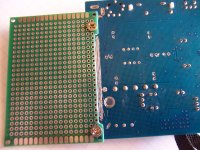
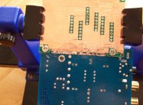
Back to through hole component output stage work. Attached below are pictures showing jumper across trace I cut out on the bottom of the board, and an area of the dac board that has been tinned with solder so that output stage board ground plane can be soldered to dac board ground plane.
Attachments
Now that is interesting. Be very curious to learn how it turns out. If you already have the LTC6655 you can see it is pretty tiny. You okay with that?
Maleetronic Voltage Reference – Maleetronic.com
Makes it a piece of cake. Even if you want to use PP caps.
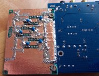
More output stage preparation pics attached below.
There are a few holes punched in the copper for the tantalum decoupling cap ground lead to come down and get soldered.
Obviously, I will have a lot of seam soldering to do a bit later.
Solder joint to dac board ground plane looks rather rough in the pic where there are shadows that look like missed spots. If examined from a good angle the solder joint looks fine.
Next step will probably be to install decoupling caps and perhaps wiring back to the dac outputs. That would be because that wiring would lay close to the ground plane and could be soldered on at the base of the socket pins. Resistors and signal caps are what will be sticking up and getting a bit crowded in places.
Attachments

Hi DRONE7, Sorry, I think we lost track of plans for you to try working on an output layout for one hour then stop. May I ask if that happened, and if so how did it go?
Yes, gave it an hour...pencil paper and eraser....used the eraser more than the pencil.
Instructive exercise.... in that I would need much more instruction to know if what I was doing was what I was meant to be doing.
All the graph paper and measuring felt just like the wallpaper days so when I peeked at your version and read that even you'd miscalculated positioning I realised how poor my efforts were going to be even given several hours application.
Edit... having just looked at the images in the post above it strikes me that I could just overlay the perfboard (I have that one) on 'some ready to etch', tape together, drill your marked holes, separate and paint on resist then etch a one off board and do away with the copper tape idea....hmmm if that's your finished layout for the i/v stage ?? I may etch this weekend.
cheers,
Bob.
Last edited:
Maleetronic Voltage Reference – Maleetronic.com
Makes it a piece of cake. Even if you want to use PP caps.
Piece of 'invisible' cake....lol
Out of stock 3.3v and 5v
@DRONE7
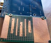
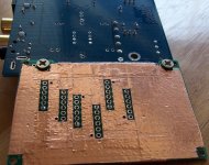
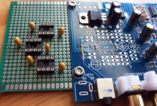
That is the socket layout, except I removed some copper from a few more holes after I took the picture so I would have some places to solder the output resistor and cap together for each channel where I mechanically stabilize them a little more than hanging out in the air (since there will be wire attached to that node going off to the audio output connectors). You don't have to do it that way, of course. There are always other ways...
EDIT: By the way, I did not miscalculate position exactly, I mis-drew position, and once I noticed it I was far enough along with the drawing that I decided I was too lazy to fix it (since I figured a note about it should suffice to warn builders).
Last edited:
Well this is the situation. I have ordered some LME49600. The footprint is the same as the LT1963. Upon removing the LT1963, the LME49600 will take its place. Placed on top of that will be an LME49710 with the pins reaching out so that the circuitry is device to device. The Solder tab on the LME49600 is Vee which will be attached to the grounding pad on the main board which is viaed to the inside ground plane of the DAC board. I will be using an LTC6655 which I received from maleetronic.com a couple weeks back. So essentially the AVCC supply will mostly be device to device with some point to point directly to the ground plane for low impedance. The soldered tab to the ground plane will provide lots of heat dissipation for the intended application with no fear of overheating and device shutdown.
Hello Mike
What do you use for the ouput capacitor 10µf ( LTC6655).
The Linear advices are : Film capacitor Polyester but the format is very large
and not smd type .
I began a small PCB and i would like to find a smd type
Thanks
Serge
Serge, I only ordered through hole 10uf output caps for LTC6655 because everybody keeps saying they can't or don't want to use SMD.
Of course SMD caps are available that are recommended for LTC665. There is a table of both through hole, *and* SMD caps in the LTC6655 data sheet they say are good. Just look up the part numbers in that table at Mouser or Digikey until you find the SMD caps you want to use.
But, if you get to use SMD, why should I have to use through hole? Never mind that. Its okay I guess. There are still some people who don't want SMD so I will use the big ones and figure out some way to make it work.
If you have trouble finding the part numbers let me know and I will try to help look them up.
By the way, it looks like the LTC6655 board Mike ordered may be using a ceramic output cap for LTC6655. I could be wrong, but that's what it looked like in the picture. If so, not recommended because of piezoelectric noise.
Last edited:
Serge, I only ordered through hole 10uf output caps for LTC6655 because everybody keeps saying they can't or don't want to use SMD.
Of course SMD caps are available that are recommended for LTC665. There is a table of both through hole, *and* SMD caps in the LTC6655 data sheet they say are good. Just look up the part numbers in that table at Mouser or Digikey until you find the SMD caps you want to use.
But, if you get to use SMD, why should I have to use through hole? Never mind that. Its okay I guess. There are still some people who don't want SMD so I will use the big ones and figure out some way to make it work.
If you have trouble finding the part numbers let me know and I will try to help look them up.
By the way, it looks like the LTC6655 board Mike ordered may be using a ceramic output cap for LTC6655. I could be wrong, but that's what it looked like in the picture. If so, not recommended because of piezoelectric noise.
If you have trouble finding the part numbers let me know and I will try to help look them up.
yes please :
In stock i have not found a good smd capa
Serge
Serge, I only ordered through hole 10uf output caps for LTC6655 because everybody keeps saying they can't or don't want to use SMD.
Of course SMD caps are available that are recommended for LTC665. There is a table of both through hole, *and* SMD caps in the LTC6655 data sheet they say are good. Just look up the part numbers in that table at Mouser or Digikey until you find the SMD caps you want to use.
But, if you get to use SMD, why should I have to use through hole? Never mind that. Its okay I guess. There are still some people who don't want SMD so I will use the big ones and figure out some way to make it work.
If you have trouble finding the part numbers let me know and I will try to help look them up.
By the way, it looks like the LTC6655 board Mike ordered may be using a ceramic output cap for LTC6655. I could be wrong, but that's what it looked like in the picture. If so, not recommended because of piezoelectric noise.
The LTC6655 will be mounted a little bit away from the LME49600/49710 for layout reasons but the reference voltage will be fed to the hybrid op amp via a short shielded cable with a ground shield. The LTC6655 carrier board will be glued to a 10uF metallized polypropylene film cap whose leads go back to the SMD pads There is a tradeoff here, piezolelectric noise versus vibrational noise from the film...in theory. ...don't know if it matters. I used this same film cap before for the bypass caps for the LT3042 and it sounded fine despite some warning about potential vibrational energy modulating the films internally. Of course the LME49600/49710 will be decoupled but this is so straightforward as the tab on the 49600 is already ground and the 49710 will be spread eagled over it ( Bend the pins out and use them for soldering parts to). If you want a fast and easy arrangement on a neat board (OPC a forum member in Canada) make a similar stereo headphone amp called " The WIRE" on a very small SMD board that utilizes both sides for components . I ordered one years ago in a group buy and sold it afterwards when I decided cans are not for me. I think it is still available from OPC in group buys.
The LTC6655 will be mounted a little bit away from the LME49600/49710 for layout reasons but the reference voltage will be fed to the hybrid op amp via a short shielded cable with a ground shield. The LTC6655 carrier board will be glued to a 10uF metallized polypropylene film cap whose leads go back to the SMD pads There is a tradeoff here, piezolelectric noise versus vibrational noise from the film...in theory. ...don't know if it matters. I used this same film cap before for the bypass caps for the LT3042 and it sounded fine despite some warning about potential vibrational energy modulating the films internally. Of course the LME49600/49710 will be decoupled but this is so straightforward as the tab on the 49600 is already ground and the 49710 will be spread eagled over it ( Bend the pins out and use them for soldering parts to). If you want a fast and easy arrangement on a neat board (OPC a forum member in Canada) make a similar stereo headphone amp called " The WIRE" on a very small SMD board that utilizes both sides for components . I ordered one years ago in a group buy and sold it afterwards when I decided cans are not for me. I think it is still available from OPC in group buys.
In fact the little PCB will be just for the AVCCL and AVCCR power supply
Serge
Serge,
Looks like almost nobody make SMD film caps. Only way to get the size down is to make the voltage rating lower. Rubycon in Japan makes some, but they are not on the LTC6655 recommended list. Don't know if they tried them or not. Digikey has some like this: 35MU106MD35750 Rubycon | Capacitors | DigiKey
Product Information: PMLCAP/Capacitor, Power Supply Units RUBYCON CORPORATION
Problem is someone would have to either buy one and measure ESR or contact Rubycon to find out since ESR is not specified for any of these film caps on the data sheets.
Other than that it looks you may have to use through hole parts. Sorry.
I would look for 'stacked' construction as they should have lower ESR. Wima seems like a good bet.
As an aside, the Rubycon film caps look very much like the film caps Allo is using in various sizes for Katana AVCC. Those and one supercap for each channel. Seems to work okay for them, at least I didn't notice any missing bass.
Last edited:
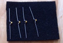
Starting to get ready for soldering multiple things together at once. Hopefully, without too much excess lead length if I can help it. Picture attached below of some 220 ohm resistors in parallel with 330pf for I/V stage feedback.
Think I can probably solder these assemblies to socket pins, with an input wire from the dac outputs soldered to one of the socket pins, and maybe then tack on a resistor to go to the filter that starts the differential output stage. Showing this and talking about it for beginners who may not have any idea about strategy for assembling things in some order. To go on a bit more then, I think I will cut off one of the leads this RC network pretty short and solder it to the inverting input pin of one of the I/V opamps. The RC network will either be standing straight up, or maybe folded over to one side, haven't decided yet. There will also be a wire from the dac output soldered on at the same time to inverting pin. I will probably tape the wire in place, then use a helping hand type of soldering holder to keep the RC in position for soldering.
Then I would plan to fold over the longer, as yet unsoldered RC lead to reach the opamp output pin and solder that in place. Later I will tack on another resistor to the long RC lead for connection to the differential stage input filter.
I will try to take some pictures as things go together in case it helps to see how the assembly process might be approached. Not the only way to do it, of course. I just hope this way works. 😱
Attachments
Last edited:
- Home
- Source & Line
- Digital Line Level
- ES9038Q2M Board