I can see how that might be the case, with having additional layers to route on.
My main thought is actually cost.
If you (or someone you know) are students, a single four layer board (up to 30 sq in) is $66
plus $20 shipping from 4pcb. This would be the best way to go at the beginning.
Otherwise you have to buy four boards, each $66 plus $20 shipping per order.
BareBones, 2 Layer & 4 Layer PCB Pricing | Advanced Circuits
At Osh Park, four layer boards are $10 per sq in and you get three of them for that rate,
so a 20 sq in board costs $200 for three copies, with free standard shipping.
No single boards, though. OSH Park ~
I would go with a single four layer board.
Last edited:
Probably, one has to expect prototypes and small runs to be costly. It would normally take a lot of volume to get down to rock bottom prices. But, hey, making is good dac is what it is.
Trying to be creative for a moment, I suppose one dac could consist of one two layer board and one smaller four layer board. The analog part of the circuitry including the dac chip itself should be four layer. Most of the basic power supply and the digital stuff can probably be done as two layer, at least if none thoughtfully. More layers is likely better though, when it comes down to best obtainable performance.
Trying to be creative for a moment, I suppose one dac could consist of one two layer board and one smaller four layer board. The analog part of the circuitry including the dac chip itself should be four layer. Most of the basic power supply and the digital stuff can probably be done as two layer, at least if none thoughtfully. More layers is likely better though, when it comes down to best obtainable performance.
Last edited:
Hi, im finally gearing up to build the AVCC supply, maybe a stupid question, but should it be build with smd components or can i use the discreet components for ease of build?
AVCC supply shouldn't have to be built with SMD parts, but maybe best to locate the regulator outputs on the back of the ground plane so they can feed directly into the AVCC filter cap pins. The idea would be to keep the impedance from the AVCC supply very low as seen by the AVCC pins on the dac chip. Compact layout and short wires can help prevent some types of noise pickup too. Only issue might depend on what you plan to use for a voltage reference for the AVCC supply. The one I used is SMD only, but I managed to solder a few of it's pins directly to the ground plane. It was really tiny though, not something I would recommend for a first SMD build. I would suggest picking a part you can work with that is as low noise as possible and filter the output as needed. Are you thinking of using an opamp based AVCC supply or something else?
i was planing to build the circuit which you have showed in the past from the below link
http://www.diyaudio.com/forums/digi...chinese-es9018k2m-i2s-dac-16.html#post5174874
i have lying around a 3.3v Voltage Regulator Module Board based on lt3042, and i thought i would use it for reference for the AVCC
i think its this one or something simular...
DC-DC 3.5V-20V To 3.3V LT3042 Low Noise Voltage Regulator Module Board | eBay
also im waiting for the krystek clock , and i already connected the src, so the project is moving a bit🙂
Victor's two opamp output stage is one way to go for that (at the link you gave), but it may not have as much filtering in as would be optimal. Still, it looks pretty reasonable.
Regarding AVCC, it is best to have two AVCC supplies, one for each channel. Otherwise channel separation suffers and it doesn't sound as good that way.
Another thing to consider is that the impedance from the AVCC supply to the dac chip not only includes the wiring from the AVCC supply to the dac chip, but also the ground return impedance from the dac chip back to the AVCC supply. That's why I like to mount circuitry on the back of the ground plane, it keeps the ground return impedance part of the power supply loop at a minimum.
To use an LT3042 to best effect, it should be used as a voltage reference that is then the input signal for a dual opamp AVCC supply. Something like a LME49720 is good to serve as the dual opamp part. I assume you have seen the circuit before and it is the one I use, one opamp section of the dual opamp chip for the left and one for the right AVCC supply.
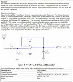
Just so we are talking about the same things, I will post the recommended AVCC supply schematics below, along with Victor's output stage schematic.
EDIT: When you linked to Victor's post, it occurs to me you could also be thinking of using LT3042 as a single supply, then use 3 x 1800uf for each AVCC channel. Although that might be very close to what Victor did, I would not recommend it for best sound quality results. AVCC turns out to be really critical and although THD @ 1kHz might look okay, it still won't sound very good in the bass and in terms of stereo as compared to the recommended supply, IMHO.
Regarding AVCC, it is best to have two AVCC supplies, one for each channel. Otherwise channel separation suffers and it doesn't sound as good that way.
Another thing to consider is that the impedance from the AVCC supply to the dac chip not only includes the wiring from the AVCC supply to the dac chip, but also the ground return impedance from the dac chip back to the AVCC supply. That's why I like to mount circuitry on the back of the ground plane, it keeps the ground return impedance part of the power supply loop at a minimum.
To use an LT3042 to best effect, it should be used as a voltage reference that is then the input signal for a dual opamp AVCC supply. Something like a LME49720 is good to serve as the dual opamp part. I assume you have seen the circuit before and it is the one I use, one opamp section of the dual opamp chip for the left and one for the right AVCC supply.
Just so we are talking about the same things, I will post the recommended AVCC supply schematics below, along with Victor's output stage schematic.
EDIT: When you linked to Victor's post, it occurs to me you could also be thinking of using LT3042 as a single supply, then use 3 x 1800uf for each AVCC channel. Although that might be very close to what Victor did, I would not recommend it for best sound quality results. AVCC turns out to be really critical and although THD @ 1kHz might look okay, it still won't sound very good in the bass and in terms of stereo as compared to the recommended supply, IMHO.
Attachments
Last edited:
i have seen the AVCC circuit from ESS as well, you think the ESS circuit would be better?
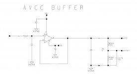
the avcc buffer (pic2) is another way for this as well?
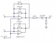
i was planing to use the circuit on the 3rd picture in your above link
the avcc buffer (pic2) is another way for this as well?
i was planing to use the circuit on the 3rd picture in your above link
Last edited:
The AVCC buffer in the second picture is the same as the AVCC supply shown in the first picture. The only difference is the second picture also shows how to use two 10k resistors and a 10uf cap to make the reference voltage for each channel. That would then be the same as the terminal labeled +1.65v in the third picture. A problem we sometimes have is that there may be more than one name for the same thing if different people have used different names for it at different times. In any case, the AVCC "reference voltage" or "offset" is equal to one half of AVCC voltage which comes out to be right around +1.65v. There is another voltage that is 3.3v which is the input voltage to each of the two opamps. Sometimes that may be referred to as a reference voltage too, but obviously it isn't the same as the 1.65v reference. The +1.65v reference is only used by the output stage, either Victor's output stage or the ESS recommended output stage (which is similar to what I used).
What I did the last time I worked on my AVCC supply was use at an LTC6655 3.3v reference for the 3.3v input to the two AVCC opamp supplies. It helps for that particular 3.3v input voltage to be very clean and low noise to start with. It is labeled DVCC in the first picture, but the actual DVCC supply is too noisy for me, so I used my own clean 3.3v chip to make that supply. An LT3042 could be used for that I guess if that is what you have available.
What I did the last time I worked on my AVCC supply was use at an LTC6655 3.3v reference for the 3.3v input to the two AVCC opamp supplies. It helps for that particular 3.3v input voltage to be very clean and low noise to start with. It is labeled DVCC in the first picture, but the actual DVCC supply is too noisy for me, so I used my own clean 3.3v chip to make that supply. An LT3042 could be used for that I guess if that is what you have available.
Last edited:
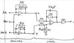
To make sure we all are seeing things the same way, the third picture above is Victor's output stage, not an AVCC circuit. For comparison, I will post the output stage I used, which is similar, but not exactly the same as the ESS circuit.
Also, to further try for more clarity, I will post a picture below showing my AVCC supply and the 'downside' part of my output stage. The AVCC components are outlined in RED color, and 'downside' output stage section is in BLUE.
Also, to further try for more clarity, I will post a picture below showing my AVCC supply and the 'downside' part of my output stage. The AVCC components are outlined in RED color, and 'downside' output stage section is in BLUE.
Attachments

Last edited:
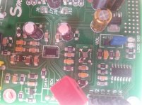
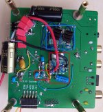
system54, Thanks for the picture, that makes it a lot easier to imagine what is going on. Since you are talking about a possible case for the clock, I assume you mean you found 100MHz (or whatever the clock frequency is, 80MHz?) noise that maybe gets smaller when you put your finger on the clock? Or maybe the big red film cap has got some clock noise radiating out of it (I hope not, but it's down in that area)?
To make sure we all are seeing things the same way, the third picture above is Victor's output stage, not an AVCC circuit. For comparison, I will post the output stage I used, which is similar, but not exactly the same as the ESS circuit.
Also, to further try for more clarity, I will post a picture below showing my AVCC supply and the 'downside' part of my output stage. The AVCC components are outlined in RED color, and 'downside' output stage section is in BLUE.
Thanks for the pics Mark
At this stage of modifications a small PCB gathering AVCC and the output stages would not it be a good idea for those who want to try this project 🙂
Serge
system54, Thanks for the picture, that makes it a lot easier to imagine what is going on. Since you are talking about a possible case for the clock, I assume you mean you found 100MHz (or whatever the clock frequency is, 80MHz?) noise that maybe gets smaller when you put your finger on the clock? Or maybe the big red film cap has got some clock noise radiating out of it (I hope not, but it's down in that area)?
i can already say that the nz2520sd (49.152mhz) sounds better than the external Clock implementation.
the case is only for fine tuning, i thing the Radiation is gone now, i will measure tomorrow.
next Project is your (ess) current stage with some z-foil 🙂
Thanks for the pics Mark
At this stage of modifications a small PCB gathering AVCC and the output stages would not it be a good idea for those who want to try this project 🙂
Serge
I would not expect an inexperienced person to build small circuits, but in my case I was inexperienced when I did it. After all, experience has to start somewhere. Prior to that I had only practiced a little with SMD soldering. Then I just decided I would try it and it turned out I was able to figure it out. Of course, I had been soldering bigger stuff for decades before trying it with SMD.
That being said, others are not me and I wouldn't expect other people to do it just because I did. However, one could still take a piece of PCB perfboard and make sure one end of it can attach to the dac board, and that end can abut up against where the bottom pins of the AVCC filter caps stick out. The perboard ground can be soldered to the dac ground plane there, and the output of the AVCC supplies can exit at that end of the perfboard and connect directly to the AVCC filter cap pins on the bottom of the dac board.
I would just suggest trying to visualize something like that one could do to try to meet the requirements for AVCC. It wouldn't have to be tiny, but it could still be a good layout and make for a good AVCC supply. In other words, a bigger AVCC supply doesn't have to be entirely on another board that sits far away from the dac board. Get them nice and snug together where it matters, where AVCC is, ground is, and power is nearby and accessible with very low resistance wiring. You get the idea, I hope. It doesn't have to look pretty, that is secondary. The main thing is that it works well.
Last edited:
Since we have recently been talking about things like possibly making a dac PCB, and like making AVCC power supplies, thought it might be of interest to see what publicly released information exists for the ES9311 AVCC power supply chip. Turns out there are at least a couple of basic information sheets for it that are not marked confidential. I will attach the two I have below in case anyone is curious about the prospect of possibly ever using one. (I also have a data sheet for it, but unfortunately it is NDA only. However, ESS is usually pretty good about providing such things through their distributors for folks willing to sign an NDA.)
Attachments
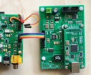
Thought I might pass along an interesting lesson I learned the hard way. I use a crimper tool and some ribbon cable to make interconnection cables as shown running between the two boards in the picture below. When the wires are small diameter as they are with the ribbon cables, I also put a dab of solder on each crimp before assembling the pins into the shells. So far, so good.
I had a wire break off right where it goes into the shell caused by repeated installation and removal of the cable. Maybe I didn't separate the ribbon wires from each other enough for best strain relief either.
Anyway, I used a little jewelers screwdriver to lift the retainer on the shell where the broken wire was, and used a little round poke tool to push it back out of the shell so I could fix it. Once out, I soldered the wire back on where it had broken and reassembled the connector.
Checked it out with a ohmmeter and it looked good. Not long after I started having trouble with DPLL bandwidth for DSD. I couldn't get the DPLL bandwidth down as low as I could before. I checked out various things including ringing out the ribbon cable again, but didn't find any problem. Among other things, I then verified with a scope that all the signals were coming across through the ribbon cable including probing at the connector or away from it on the circuit board traces. Signals looked good. No problem found.
But there was one funny thing, if put my finger on the cable, or near it on the circuit boards I could change the DPLL lock-in-ability.
To make an even longer story short, I took apart the connector and looked at it carefully with a microscope. For the pin insert I removed to re-solder (female), the springy contact points were not as tight as they used to be. Very careful examination showed there was contact, but the contact force was very small, more of a sliding fit than an interference fit.
As it happens pin header pins are .025" square. The poke tool I used to push out the pin was found to measure at .032" which evidently was enough to permanently deform the contact point's springiness on the female pin insert, but only slightly. The result was that there was a connection that measured fine every way I had to measure it, but was now apparently somewhat noisy.
Made up a new cable and connector assembly, problem fixed. Also made a poke tool that measures .023" round. It works fine, verified it causes no permanent contact deformation with microscope.
Attachments
Last edited:
I suppose that some of you might have seen this new IC from the TI catalogue that seems to take a special place in their line of audio op amps:
INA1620 INA1620 High-Fidelity Audio Operational Amplifier With Integrated Thin-Film Resistors | TI.com
(See also the relevant discussion in the forum around 08.08 - New Audio Op Amp - OPA1622 and following).
There has also been a growing amount of enthusiasm surrounding the use of OPA161x in the I/V stage in Mikett's ES9028Pro thread. And Markw4 mentioned the line being used in the ES9038PRO evaluation board.
Aside from the horrific WQFN24 format is there an obvious reason why this one could not be applied as the differential amplifier in the output stage, taking the advantage, quite obviously, of its matched 1k resistors . I guess that one could try and solder it to a qfn to dip adapter and move on from there with, for example OPA1612 in the I-V, followed by the INA1620. Might even work directly as a headphone amplifier. If so, what would determine the proper R and C values in the differential stage - could one just follow "blindly" the evaluation board design (INA1620EVM INA1620 Audio Operational Amplifier Evaluation Module | TI.com? Or a little more thought would be needed for optimal performance - as suggested by the numerous modifications of the output stage, suggested in the previous pages of this thread?
Good question about opmaps for dac output stages. It could be that LME49720 is hard to beat so long as it can supply the necessary output current. For ES9038PRO a higher current capability opamp was needed and the next best choice was probably OPA162x.
The problem is there are really two problems. One is the designing an output stage that looks like a good choice on a schematic and in simulation. The other problem has to do with a mostly unseen problem which is the RF leakage coming out of the dac outputs. Output stages are designed to finish the reconstruction process started with the last interpolation filtering inside the dac, but the output stage has to deal with some very HF content. That means the opamps have to be able to tolerate some unquantified RF/HF junk that can potentially get amplified to the point it can then get demodulated in semiconductor junctions and cause shifting bias voltages which in turn generate distortion that may be hard to characterize because it can be maybe kind of non-stationary.
And of course, even if we can find some opamps that can handle the HF junk well and be tolerant of it while they are being used to help filter it out, there is the question of whatever remaining HF junk may make it into a power amp and what it might do to the sound there.
All this is nothing new, people have been thinking about it for a long time, but it is one of those things that may be hard to model so cut-and-measure methods may be what we are left with.
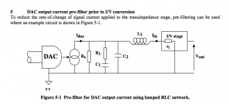
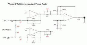
In that regard I will post some output stage schematics below that maybe can help illustrate.
Unfortunately, I can't finish saying everything that has been on my mind recently about this stuff, but I will try to pick it up again a little later.
The problem is there are really two problems. One is the designing an output stage that looks like a good choice on a schematic and in simulation. The other problem has to do with a mostly unseen problem which is the RF leakage coming out of the dac outputs. Output stages are designed to finish the reconstruction process started with the last interpolation filtering inside the dac, but the output stage has to deal with some very HF content. That means the opamps have to be able to tolerate some unquantified RF/HF junk that can potentially get amplified to the point it can then get demodulated in semiconductor junctions and cause shifting bias voltages which in turn generate distortion that may be hard to characterize because it can be maybe kind of non-stationary.
And of course, even if we can find some opamps that can handle the HF junk well and be tolerant of it while they are being used to help filter it out, there is the question of whatever remaining HF junk may make it into a power amp and what it might do to the sound there.
All this is nothing new, people have been thinking about it for a long time, but it is one of those things that may be hard to model so cut-and-measure methods may be what we are left with.
In that regard I will post some output stage schematics below that maybe can help illustrate.
Unfortunately, I can't finish saying everything that has been on my mind recently about this stuff, but I will try to pick it up again a little later.
Attachments

Last edited:
I would not use a 1622 on the last stage because you would not be using it to its strengths. High currents at high voltages...like driving headphones where as the output voltage increases, the currents demanded increases. Its strength is also the ability to handle complex impedances that some headphones will give. There is no way the IV circuits demand 80ma RMS output currents.
The OPA1622 is conceptually a similar headphone circuit that Mark recommends. The one he recommends is essentially what is called a composite op amp where the first op amp provides all the voltage gain necessary and does not stress the output stage because it is driving another op amp with a high impedance. The second op amp is akin to a power op amp where it is used with a gain of 1 but can supply the current required. The output feedback wraps back into the first op amp. Thus a composite or hybrid op amp. My preamp is based on this but it goes one step further in that the first IC has output pins that bypass the output stage of the op amp thus completely bypassing an unecessary stage before it feeds the second power op amp.
The OPA1622 attempts to provide most of what that does in a simpler format into one chip. Like everything it is give and take. One give is simplicity and one take is a little performance.
The OPA1612, however has a wimpier output stage as compared to a 1622 ( but better voltage performance) but a much more stout output stage than a LME49720. Maybe this matters some in the IV circuits shown above. Try them and report back.
Last edited:
Oops! Typo that needs correction in my last post. I said, "For ES9038PRO a higher current capability opamp was needed and the next best choice was probably OPA162x." That last opamp part number should have been, OPA161x instead.
Anyway, as I keep suggesting to people, do as I say and not as I do, particularly when it comes to output stages. Proper filtering is important at the output stage and I may have to go back and do some more work on mine to make it better. In addition to the caps shown in the schematic attached below, just as something easy to try, I added some 1/8" stereo extension cables between the mini phone plug output on the dac board and the analog line input on the DAC-3. It sure sounds like 30' of extra cable smooths out the high frequency cymbal sounds some. Obviously, there is some capacitance and inductance that could be attenuating any remaining RF coming out of the dac board. Even 15' has some effect. Haven't fully figured out if there is some lumped equivalent I might use, or if I simply could use some more HF filtering upstream of dac output, specifically somewhere in the output stage.
As I have pointed out before, I don't have any proper audio distortion test equipment here, and even getting a sound card and notch filter to work has proven troublesome and is still not fully functional.
Probably there is a chance I could borrow some really good audio test equipment, but just I don't like borrowing other people's cherished stuff. Also, I don't know how long I want to keep optimizing this dac project. It has been interesting so far, but I don't want it to become like a job. Besides, the modded dac sounds pretty good, actually. Not quite at DAC-3 level, but good enough I think I could be satisfied with it (and I am very picky about dac SQ as I think people probably mostly already know).
Attachments
Last edited:
- Home
- Source & Line
- Digital Line Level
- ES9038Q2M Board