I used (these) in Quasimodo V4 and they worked well for me. It pleases me that their mechanical drawing reminds readers the terminals are square, 25 mils on a side ... encouraging designers to calculate the length of the diagonal (25 x sqrt(2)) to obtain the final diameter of the drill hole after plating. The resulting number was just about identical to the lead diameter of a medium wattage thru-hole resistor (like this one). So I just copied the pad size and drill size from my medium wattage resistor component, over to this 1-pin-connector component, and the result was success. At least for me.
One way to perform square wave Iload testing is with two resistors and a switch.
When the switch is open, Iout = 1% of Iload_max. When the switch is closed, Iout = 99% of Iload_max. If the switch's risetime and falltime are very fast (giving, say, greater than 400kHz bandwidth in the {risetime - bandwidth equivalency formula: tR = 0.34/BW}, then the resulting Iload waveform can be considered a "square" wave. Fortunately, power transistors with appropriate predriver circuits, can perform excellently in this application, giving very high speed switches with very short rise/fall times. Either BJTs or MOSFETs.
One way to perform square wave Iload testing is with two resistors and a switch.
R1 = Vout/(1% of Iload_max)
R2 = Vout/(98% of Iload_max)
R1 goes from Vout to Gnd, and R2 goes from Vout to switch to Gnd.
R2 = Vout/(98% of Iload_max)
R1 goes from Vout to Gnd, and R2 goes from Vout to switch to Gnd.
When the switch is open, Iout = 1% of Iload_max. When the switch is closed, Iout = 99% of Iload_max. If the switch's risetime and falltime are very fast (giving, say, greater than 400kHz bandwidth in the {risetime - bandwidth equivalency formula: tR = 0.34/BW}, then the resulting Iload waveform can be considered a "square" wave. Fortunately, power transistors with appropriate predriver circuits, can perform excellently in this application, giving very high speed switches with very short rise/fall times. Either BJTs or MOSFETs.
Ok I think that is exactly the same part (but with the one I linked to is showing stock availability). Your calc is consistent with the data sheet which recommends 0.89mm diameter when plated. Cool. (Thanks for the reminder that they are square and implications for hole size.)
I have added wire pad holes (1.6mm outside and 0.9mm internal diameters) for these. Should be ok. Things are now a little cramped but given these pins sit vertically it shouldn't be a problem. I also did the same for my 5V and GND "test points".
Thanks also for the guidance re square wave load testing. I will circle back to this when I have the boards.
Latest version attached. Hopefully this is looking ok and I can turn my attention to the power rails and current controls.
I hope I can solder C4 - it will be the smallest part yet. I've extended the pads to make things easier (as I did with the 100nF surface mount caps) - time to learn frying pan surface mount soldering I guess…
Cheers
Steve
Attachments
For Test connectors I use tinned copper wire about 0.4mm to 0.5mm diamter turned into a loop about 2mm diameter and the two ends inserted into a 0.8mm hole and soldered. A squeeze with pliers will deform 0.5mm enough, so that a pair will fit a smaller hole.................For the test connectors, do you mean breakaway headers like these and 0.8mm wire pad holes to fit them in?............
That way you can "hook on" a probe for safe measuring.
I prefer a force fit for pins like this so that I can set them to height and know they won't move during handling/soldering..............reminds readers the terminals are square, 25 mils on a side ... encouraging designers to calculate the length of the diagonal (25 x sqrt(2)) to obtain the final diameter of the drill hole after plating. ............
The corners of the squares "dig in" to the sides of the hole, whether plain fibre, or plated through.
I can usually adjust the pin to exactly 90° to the PCB face if the PCB is not too thick.
A really stiff "force fit" can be adjusted with a pair of long nose pliers.
or use a little glue to set the pin prior to soldering it permanently in place
Ok so I am now working on the main power supply boards, looking at low RDSon NMOS pass transistors and I come back to my question regarding soldering.
While choosing between them may be polishing the proverbial, I need to pick one and run with it. Should I just forget about D2Pak? 😱
Ok so I am now working on the main power supply boards, looking at low RDSon NMOS pass transistors and I come back to my question regarding soldering.
How difficult is it to hand solder a D2Pak or D2Pak 7 Pin package. Is it possible with the drain tab? I want to learn how to do "skillet SMD soldering" but would like to be able to fall back to hand soldering if I find I am mess in things up. This will help me choose the NMOS transistors (IRF1324S 1.0mR max Rds(on) D2Pak 7 Pin; IRFS7430 1.2mR max Rds(on) D2Pak, TO-262, TO-247AC, TO-220; IRLS3813 1.95mR max Rds(on) D2Pak, TO-220AB; IRF8252 2.7mR max Rds(on) SO-8 etc.)
While choosing between them may be polishing the proverbial, I need to pick one and run with it. Should I just forget about D2Pak? 😱
Actually, ignore my question above. Unless I have missed something, I will run with IRF8252. It has Max Vds = 25V and Id = 25A which would seem to be plenty; Max Rds(on) = 2.7mR; easy to solder SO-8 package (as noted by Mark some time ago) and Max Power Dissipation of 1.6W @70C which is more than enough headroom for the 67.5mW I will need. Less than half the price of the IRFS7430 which, while it has higher ratings in a number of areas, it isn't worth focusing on the lower Rds(on) (1.2mR) given the potentially more challenging D2PAK package (although I note my thermal demands are such that reflowing solder all the way under the drain tab likely isn't critical).
I copied the slope of the "10 msec @ high VDS" piece of the Safe Operating Area curve, and positioned it with approx the same spacing as the other curves.
When the switch finally gets the okay to "commence soft start", the MOSFET drain is at Vsupply (12V, 5V, 3.3V) and the MOSFET source is at 0.00 volts, so Vds = 12 or 5 or 3.3 volts. Notice the permitted Ids. Cowabunga!
Of course, they plot the curve for a worst case temperature scenario so you get that margin-of-safety back. But still: owww!
Attachments
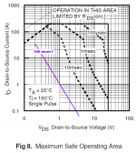
Hmmm... so she blows. So I understand, the 100ms comes from where? As the output caps charge, Vs rises, Vds falls and so does current. I know the formula for Vc as a function of supply voltage (in this case Vd) but... (Also, when I look at the same chart for the IRFS7430 is has a curve for "DC" - what is meant by this?)
I also see that with Vd of 12V and the VOM1271 at 20mA current providing Voc of 8.7V then a Vgs limit of 20V isn't enough...
I will look again for more suitable parts. Thanks. 😱
I also see that with Vd of 12V and the VOM1271 at 20mA current providing Voc of 8.7V then a Vgs limit of 20V isn't enough...
I will look again for more suitable parts. Thanks. 😱
I also see that with Vd of 12V and the VOM1271 at 20mA current providing Voc of 8.7V then a Vgs limit of 20V isn't enough...
Ignore this bit...and this bit...
(Also, when I look at the same chart for the IRFS7430 is has a curve for "DC" - what is meant by this?)
Last edited:
Ta=25°C in that plot tells you that the device is tested without a heatsink and that at the start of the pulse the Tc also equals 25°C...........................
Of course, they plot the curve for a worst case temperature scenario so you get that margin-of-safety back. ................
That is the best case for junction temperature.
If Tc starts higher due to previous history of dissipation, then the permissible currents go down according to the temperature de-rating, usually specified in the datasheet.
That plot also shows that this mosFET is affected (quite severely) by second breakdown.
Many here deny this can happen for mosFETs.
Try plotting on the 1.6W curve (straight line). This would be the DC line.
This new line clearly shows that the 100ms guesstimated line cannot be correct.
Then try estimating where the second breakdown knee happens.
note that the second breakdown knee is shown:
100us - 17Vds
1ms - 5Vds
10ms - 0.5Vds (not the second knee @ 1.1Vds)
Last edited:
Hmm, Tambient = 25 C and Tjunction = 150C according to the plot legend.
Sounds like they put the parts-to-be-tested in a preheater at 150C, to stabilize TC = TJ = 150C. Then when the loader machine slides a part into the DUT socket, sounds like they turn on the Thermostream (semiconductor tester air blower {LINK}) at 25C during the test. Voila, Tambient = 25C and Tjunction = 150C.
Methinks SGK may wish to calculate a tighter upper bound upon C_Load_max, thus giving a better estimate of I_soft_start and T_soft_start. Perhaps a feasible and not-disgusting design may exist, having I_soft_start < 0.5 amperes. Perhaps it may involve bolting a TO-220 package + low profile heatsink, to the PCB. Bolt goes thru board, heatsink, and TO-220. (example)
Last edited:
Hi
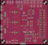
I spent a few hours today working on the PSU board (work is slow). See attached draft. I still have a few things to do e.g. I should remove the resistor values for parts that will depend on desired output voltage. C8 is a placeholder for now.
I also looked at the datasheets of various International Rectifier N-MOSFETs and their max safe operating areas. I understand that a DC curve is for continuous current (rather than pulsed) and looking at this curve is a safer thing to do. If the FET can handle 12Vds + 5A continuously then it should be fine (?) assuming I manage to curb the in-rush appropriately.
From this exercise, it seemed that making the leap to a D2PAK was worthwhile (or even necessary). With minimal Rds(on) and only up to 5A of current, thermal considerations would seem very manageable. Take, for example, the IRFS7437. Unless I am missing something (and I probably have 😱 ) thermal resistance junction to ambient is 40C/W and so, using worst case Rds(on) of 1.8mR and full 5A rail current, that's only 45mW of power dissipation for a mere 1.8C rise from ambient. Also, while Fig 10 requires some estimation of safe operating area for a 12V Vds, looking at the DC curve it would seem 5A is "ok" ?
I tentatively put forward my draft for scrutiny....
Steve
PS: One question about traces for smoothing caps. I have always thought of current flowing into the caps sequentially (C1 fills and then C2) and hence the trace must go to C1 before continuing to C2 and on from there. Hence I have the trace snaking through the board. This wouldn't seem consistent with power planes, however, and so I'm questioning whether this is correct...
Attachments
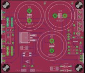
Just in case it wasn't obvious:
- the plan is to mount the rectifier diodes and LT1084 on the enclosure
- AC Out is intended to provide a junction to share the AC secondaries with another board should it become necessary/desirable. I'm not sure I have enough gap between them to allow two insulated Faston connectors... Also, would I need the snubber on the second board?
Rather a surprising schematic.
AC -> rectifiers -> two electrolytic filter caps -> MOSFET switch -> no caps at all -> LT1084 voltage regulator -> one electrolytic filter cap -> +5V output
I was under the impression your goal was to put the switch(es) downstream of the regulators, so that the voltage dropped across the switches immediately reduces the regulated output voltage by (Iout x Rds_on).
No that was the problem I encountered and sought to avoid.
Originally, I had the 5V (and 12V and 3.3V) power rail and no standby 5V. This was because I couldn't figure out how to have the switches triggered by anything other than PWR_OK i.e. the main power rails and regs were always 'on' and the switches would have sat on the other board with the TPS3510.
I was then introduced to the issue of Rds(on) and I thought it foolish to invest in regulated power rails only to (intentionally) introduce a load-dependent resistance after regulation. (Now if that is just a couple of milli amps perhaps it's a non-issue...)
(With help here) I then managed to get the switch trigger to be FPO low (or at least I think it works). So now PWR_ON signal comes in, FPO goes low, the power rails are 'turned on' (current flows from the initial smoothing caps to the regs and output cap) by the 5VSB and TPS3510 "control board", the rails come up to spec voltage and then the TPS3510 sends a PWR_OK signal to the motherboard. Probably more like what's meant to happen. Rds(on) now sits before the regulators which can combat its (now minimal) resistance. One problem with this setup is that when the power rails are meant to be turned off there's still the charged output cap. The advantage is that the switch and gate cap regulate the initial in-rush through the regulator.
Well, that was the thinking... Am I smoking dope?
Last edited:
Since the apparatus seems to be mains-powered, there's very little reason not to install a 10 ohm, 10 watt resistor across the +5V supply. This will discharge the (C_Load < 13 milliFarads) +5V supply in less than 40 milliseconds.
Similarly, a 47 ohm, 10 watt resistor across the +12V supply will discharge it right smartly. And a 10 ohm, 5 watt resistor across the +3.3V supply will get the job done there too.
Yes, these resistors needlessly burn power. Compared to 5 amps of load current, is it anything to worry about?
Maybe you could install a transistor in series with each of these resistors, turned on or off by some variant of "wakey uppie and do your jobbie" control signals.
The device starts at Ta & Tc & Tj = 25°CHmm, Tambient = 25 C and Tjunction = 150C according to the plot legend.
during the pulse, Tj rises to 150°C.
That increase in temperature is dependent on the power dissipated and the dynamic Thermal conductivity.
For very short pulses with a low duty cycle the thermal conductivity is enormous, even without a heatsink.
That's why you see typical duty cycles of <=3%. to allow time for Tj to return to 25°C before the next pulse arrives.
Thanks Mark. Presumably it's the big fat output cap that needs to be discharged rather than the estimated motherboard capacitance and presumably the two filter caps should be trickle discharged (over a longer period) when/if the mains power is disconnected. This is the origin of my question in post #52.
But first, can we come back to in-rush as I think my understanding of this may well be fundamentally flawed. The AND9093 document, your post #32 and "with inrush-current limited to < 5A" from #36 led me to believe that both the pass transistor and the (LT1084) regulators needed to be protected from the in-rush to charge the motherboard capacitance and any output caps post regulators on the main power rails. This, together with the discussion regarding Rds(on), led me to believe that any power rail switch and its voltage slew-rate control had to be before the regulators - even if I were insensitive to the impact of Rds(on) on output voltage - and limited to, say, 5A i.e. within the capability of the regulators. Commensurately, if the switch and slew-rate control were before the regs then the power rail output capacitance needed to be added to Cload calculations when determining the cap to ground added to the gate of the pass transistor for voltage slew rate control.
I read the LT1084 data sheet once more. The description of current limiting is unclear to me, likely because it is so basic and well understood by all but me. So here goes another basic question. Does the LT1084 have managed current limiting or does it just shut down if the threshold is exceeded? I was thinking the latter. If the former, however, presumably I don't need to worry about the in-rush through the regulators and simply need worry about the in-rush only in so far as the safe operating area of the pass transistor isn't exceeded. (And if I were insensitive to Rds(on) impact on output voltage because it was very small with an appropriately selected pass transistor I could even then place the switches after the regulators and output caps and on the TPS3510 board rather than on the power supply boards...5A need not necessarily be the upper limit to the in-rush current limiting...Bleeder resistors on the power rails would bleed all the caps when the mains power was disconnected...etc)
Capacitive load. Section 3.2.8 of the ATX Power Supply Guide ver 2.2 (pdf) provides guidance which is helpful as their guidance is less than an overly conservative 13.2mF :
An externally hosted image should be here but it was not working when we last tested it.
Last edited:
Inrush current @ startup is only a concern, if either
One of the well understood, standard, widely discussed inrush-circuit-idioms appears in your design: diode bridge D3-D6 followed by capacitor bank C1-C2. SPICE will tell you that after switch-on, the first two cycles of AC mains power will see monstrously enormous diode currents, as the transformer secondary attempts to drive the dead short that fully-discharged C1 and C2 present. These enormous currents flow through the diodes and through the capacitors' ESR. Comparing the SPICE waveforms to the component datasheet absolute-max-specs, might or might not suggest a parts upgrade.
Non-standard designs, however, may not have a mountain of accumulated analysis and experience. Brand new analysis and simulation is required. Fortunately this is not difficult, merely tedious. Just simulate a power-on dead start, plot the currents through all components, and plot the power dissipation (LTSPICE red/green thermometer icon) of each component. Repeat for a few different "at what phase of the AC mains sinewave did the user flip the ON/OFF switch" angles (perhaps: 0, 30, 60, 90, 120 degrees ??). How bad are the worst-case current waveforms? How bad are the worst-case (power dissipation vs. time) plots? Do you violate a component's ratings by a wildly excessive amount?
Repeat for power-off, if you deem that necessary.
If everything looks good and margins-of-safety are high, you're done. If not you may want to substitute better-spec parts. Or maybe the situation is so grave that you need modify the design to something that gives, by design, dramatically lower inrush current.
You won't know what you need to change, until you've simulated what you've got.
- the current through a component wildly exceeds its ratings, or
- the power dissipated by a component (P = I x V) wildly exceeds is ratings
One of the well understood, standard, widely discussed inrush-circuit-idioms appears in your design: diode bridge D3-D6 followed by capacitor bank C1-C2. SPICE will tell you that after switch-on, the first two cycles of AC mains power will see monstrously enormous diode currents, as the transformer secondary attempts to drive the dead short that fully-discharged C1 and C2 present. These enormous currents flow through the diodes and through the capacitors' ESR. Comparing the SPICE waveforms to the component datasheet absolute-max-specs, might or might not suggest a parts upgrade.
Non-standard designs, however, may not have a mountain of accumulated analysis and experience. Brand new analysis and simulation is required. Fortunately this is not difficult, merely tedious. Just simulate a power-on dead start, plot the currents through all components, and plot the power dissipation (LTSPICE red/green thermometer icon) of each component. Repeat for a few different "at what phase of the AC mains sinewave did the user flip the ON/OFF switch" angles (perhaps: 0, 30, 60, 90, 120 degrees ??). How bad are the worst-case current waveforms? How bad are the worst-case (power dissipation vs. time) plots? Do you violate a component's ratings by a wildly excessive amount?
Repeat for power-off, if you deem that necessary.
If everything looks good and margins-of-safety are high, you're done. If not you may want to substitute better-spec parts. Or maybe the situation is so grave that you need modify the design to something that gives, by design, dramatically lower inrush current.
You won't know what you need to change, until you've simulated what you've got.
Thanks Mark. Yes I knew I had to model everything but my question was much more generic. That is, when an IC such as the LT1084 has current limiting what does this mean? Active limiting to ensure current doesn't exceed XYZ or shutdown if current exceeds XYZ? (When I look at current through the LT1084 in LTspice it suggests the former.) The reason for the question is that if the regulator provides current limiting then presumably there's no need to throttle the voltage slew rate of the pass transistor if the current limiting of the regulator is sufficient to keep the pass transistor within its safe operating area.
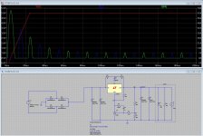
I've redone the stability, PSRR, output impedance and transient analyses for the 5V power supply with the larger caps. I did not, at this stage, insert the pass transistor into the analysis but will do so. The LT1084 (rather than LM317) and the larger filter and output caps implied a different value for R4 in the circuit (16.2k rather than 47k) and the peak output impedance seemed to benefit from the addition of a 470uF output cap after the large one (albeit this peak is at circa 200kHz - should I care at all?). Adding the additional output cap altered stabilisation and hence R4. I will post a link to the results of this work later.
Current flows. I had also modelled an AC source plus rectifier diodes as I am also aware of the points you raised above. I could not find a model for the 30A FFPF30UP20STU diodes I was planning to use (and which you had once recommended to me). I did find a model for their 20A equivalent, the FFPF20UP40S, and have used that for now.
The results of this are strange and perhaps I am doing something incorrectly. Or perhaps the modelling is correct and highlighting a problem with the circuit. See attached.
Even with just a 1.15A load the current through the diodes settles at 7A peak. Yes, there's the in-rush as the caps are charged but this appears to be within the peak limits. (The FFPF20UP40S have a non-repetitive peak surge current 60 Hz single half-sine wave absolute maximum rating of 200A while for the FFPF30UP20STU it's 300A, as I am sure you are already familiar with.) The one exception to this is the second wave through D4 but this would be below the repetitive peak limit of the 30A version.
So this doesn't seem like a good foundation for looking at current through the filter caps - unless of course a problem with the filter caps is indeed the cause! When I look at current through the LT1084 I see it rising sharply after a few milliseconds to a touch over 6A (limited by regulator?), presumably as the output caps are charged, before falling to 1.16A (with a 1.15A load) after about 26ms.
The 25V (29V surge) caps I have are rated as follows:
- rated ripple IR~ at Tmax and 100Hz: 5.4A [the R is not presented as a subscript]
- nominal current IR for 5 min 3300uA
- ESR at 100Hz 14mOhms
- Tan at 100Hz 20
What is the right way to interpret the first 2 and 4th?
(BTW I am using these caps at the moment in a 12V supply. Transformer-> full wave bridge (Cree Sic diodes) -> two caps as filter -> 12V regulator -> one cap.)
Regards
Steve
Attachments
- Status
- Not open for further replies.
- Home
- Amplifiers
- Power Supplies
- Enough current to turn on 3 mosfets?