yea i came across this thread a while back i meant to keep up to date but....
ive had some experience with powering mobos that dont require atx power supply management
sq wise we have discovered that a few things helped
using a transformer, bridge and reg per rail
using separate/additional 5v rail each for ssd/music drives
separate 12v rail for 12v on the 24pin (i think cpu noise gets in)
even power in a usb port will have gathered noise
separate 12v rail for 12v on the 24pin (i think cpu noise gets in)
This doesn't make sense to me. If one has a very good 12V source and both locations take 12V with a common reference (GND) how can noise it be that noise pollutes the '12V system' or, rather, how can it be that provision of independent 12V rails to two points sharing the same reference be better?
Doesn't the noise have to circulate via the GND reference and not back through the supply line? If so then two separated supply lines isn't going to achieve much.
If indeed there is some sort of noise from one user of the 12V polluting the 12V system then surely it makes more sense to filter the 12V feed so that noise from the item it is powering can't travel up the 12V supply line and affect other 12V-powered components.
And I wonder what such a filter or blocker might look like... Simple diodes restricting the flow of current to ensure no 'back eddies' - even if that's even possible - or something more complex?
SoTA do a great trade in a device which purports to filter the power to an SSD and restrict any noise from the SSD from circulating back into the PSU. We discussed this in another thread and Mark mentioned the potential for device noise to couple back to the supply side through typical protection diodes (and I followed his advice when I built my first little 5V regulator for an SSD bank, using two diodes in series with a cap to GND between them).
well we tested lots of different stuff lots of stuff did not affect the sq the way we wantedThis doesn't make sense to me. If one has a very good 12V source and both locations take 12V with a common reference (GND) how can noise it be that noise pollutes the '12V system' or, rather, how can it be that provision of independent 12V rails to two points sharing the same reference be better?
never dwelled much on the science of it just experimented and went with what sounded best
as far as the 12v i imagine that the cpu has fast transient loads that does the harm
Doesn't the noise have to circulate via the GND reference and not back through the supply line? If so then two separated supply lines isn't going to achieve much.
If indeed there is some sort of noise from one user of the 12V polluting the 12V system then surely it makes more sense to filter the 12V feed so that noise from the item it is powering can't travel up the 12V supply line and affect other 12V-powered components.
And I wonder what such a filter or blocker might look like... Simple diodes restricting the flow of current to ensure no 'back eddies' - even if that's even possible - or something more complex?
SoTA do a great trade in a device which purports to filter the power to an SSD and restrict any noise from the SSD from circulating back into the PSU. We discussed this in another thread and Mark mentioned the potential for device noise to couple back to the supply side through typical protection diodes (and I followed his advice when I built my first little 5V regulator for an SSD bank, using two diodes in series with a cap to GND between them).
we had a sotm sata filter
didnt like it
id prefer not to have the problem rather than trying to cure it
dunno why the multiple powersupplies work well
could be because it splits up the current load
Well I finally got my power supply working and had the three voltages to connect to this TPS3510-based board to see if it works. Standalone it seems to behave as it should, however it is not doing so when connected to my motherboard.
Powered on but unconnected to the motherboard, the voltages at the TPS3510 pins all look correct. (Measurements taken with my very cheap DMM.)
Pin 1 PGI measures 2.7V (50% of the 5V voltage)
Pin 2 GND
Pin 3 FPO held high at 4.0V
Pin 4 PSON held high at 3.4V
Pin 5 VS3.3 measures 3.6V
Pin 6 VS5 measures 5.45V
Pin 7 VDD connected to 12V rail measures 12.15V (12V rail voltage less drop over Schottky diode B130B)
Pin 8 PGO held low at 0.1V
If I short PSON to GND, to emulate a 'give me power' request from the motherboard:
Pin 3 FPO goes low and the LED indicator lights
Pin 8 PGO goes high to 5.5V
The VOM1271 turn on the pass transistors and 12V/5V/3V3 is supplied to the 24-pin and 4-pin connectors.
All great.
However when it is connected to my motherboard, FPO goes low for a fraction of a second on psu power-on as the LED flashes on momentarily, FPO is then held high at 4V, PGO is kept low while PSON measures 0V. It's as if fault protection is latched and hence despite PSON being low, no power is being delivered and PGO is kept low. But the rail voltages are good and hence a fault protection latch should not occur.
Also, just on PSU power-on the motherboard should not be asking for power by sending PSON low. PSON should stay high until the front panel button is pressed to turn the computer on. [When PSON goes low on such event and the rail voltages are at spec (which they are) then (as noted above) FPO should go low, the LED light and PGO (power good) go high.]
All a bit frustrating. Perhaps the motherboard is the issue but it did for awhile continue to boot with my picoPSU. In my dicking around I now seem to have the motherboard locked in some sort of sleep state as now the front panel LED just blinks and it won't boot up even with the picoPSU. I continue to grapple with it.
So....
While I try to figure this out I would like to test the measurement amplifier which is built onto the board and take a look at the incoming voltages. I presume I use my scope's FFT function to do this but I have never used this before. I know I need to look at the ground noise floor first. We built in a CTS208-4 dipswitch to select between GND, 12V, 5V and 3V3 for measurement. I will have to see if my scope can store the result from reading GND while displaying the new measurement for one of the voltage rails. Any tips on how to do all this properly would be greatly appreciated.
Attachments
Last edited:
I have no advice to offer about anything except your last two lines, waveform overlay.
My Rigol 2000-series digital scope offers Store->Trace and Store->Waveform features. I used one or the other of them, don't remember which, and it got the job done beautifully.
My interpretation, which could be wrong, is this: You store a scope screenshot onto a USB Thumbdrive. That becomes, in effect, the backdrop for subsequent scope usage. It's the canvas that new waveforms are painted upon. So you store NodeA, then change your hardware setup, then probe NodeB. Voila, the B waveform appears on the scope face along with the A waveform. BEWARE, don't change the horizontal sweep rate between A and B. Also if possible, don't change the vertical gain (volts/division) -- it will "work" but you will find the result confusing, I predict. If possible, don't change anything except vertical position -- shifting waveform B up or down so it doesn't overlay and occlude waveform A.
Thanks. I'll figure it out.
I watched a couple of online videos regarding using FFT on a 'scope. Perhaps before I move to overlays I can check my basic FFT use/interpretation.
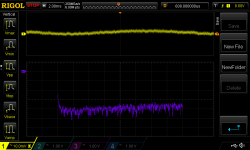
The attached pic is a measurement of the 12V rail. I chose to bandwidth limit the channel to 20MHz. I understand it is good to put the extra samples to use by switching the scope to "high res" mode under Aquire. The vertical resolution of the voltage waveform is 10mV per division, the lowest my scope will go, and the coupling is AC. (The horizontal division for the voltage waveform changed as I changed the horizontal division for the FFT.)
For the FFT, I selected (for now) 2.5kHz per division. My scope only uses 8 of the 10 display divisions for FFT. So this is a range from DC to 20KHz and the centre of the display is 10KHz. Vertical resolution was 20dB per division and I used a vertical offset of 60dB. I left the Window at the default which is Rectangle.
I know there isn't a noise floor reference to see yet but I'm wondering how to interpret what I see here (i.e. very basic stuff). My LTspice model of the measurement amplifier suggests amplification of 48.9dB with -1dB points of about 13Hz and 165kHz. So any noise on the 12V supply between these two frequencies is being amplified some 278x. If I eyeball the scope image I see that generally speaking that the amplified noise is down, say, between 70 and 90dB. So do I add the dB amplification to the -70-90dB?
More generally, am I doing things correctly thus far?
I watched a couple of online videos regarding using FFT on a 'scope. Perhaps before I move to overlays I can check my basic FFT use/interpretation.
The attached pic is a measurement of the 12V rail. I chose to bandwidth limit the channel to 20MHz. I understand it is good to put the extra samples to use by switching the scope to "high res" mode under Aquire. The vertical resolution of the voltage waveform is 10mV per division, the lowest my scope will go, and the coupling is AC. (The horizontal division for the voltage waveform changed as I changed the horizontal division for the FFT.)
For the FFT, I selected (for now) 2.5kHz per division. My scope only uses 8 of the 10 display divisions for FFT. So this is a range from DC to 20KHz and the centre of the display is 10KHz. Vertical resolution was 20dB per division and I used a vertical offset of 60dB. I left the Window at the default which is Rectangle.
I know there isn't a noise floor reference to see yet but I'm wondering how to interpret what I see here (i.e. very basic stuff). My LTspice model of the measurement amplifier suggests amplification of 48.9dB with -1dB points of about 13Hz and 165kHz. So any noise on the 12V supply between these two frequencies is being amplified some 278x. If I eyeball the scope image I see that generally speaking that the amplified noise is down, say, between 70 and 90dB. So do I add the dB amplification to the -70-90dB?
More generally, am I doing things correctly thus far?
Attachments
PS: I get a "function limited!" message when I try to save the MATH output as a Reference. I can save the channel/voltage waveform but not the MATH even though the option is selectable and the ability to do so is described in the manual. I will contact Rigol UK on Monday.
I have attached a scope pic of the GND. The 12V FFT is going to virtually overlap the noise floor FFT.
I have attached a scope pic of the GND. The 12V FFT is going to virtually overlap the noise floor FFT.
Attachments
Mark
Could there be an issue when this amplifier is amplifying its own supply voltage? The reason I ask is because I looked at some crude Vpp and Vrms measurements with my scope. With a constant time division (2ms) and vertical division (500mV) I measured the output of each supply rail at each regulator output and then at the output of the amplifier. At the regulator outputs, the measurements were basically the same (14mV RMS and 20Vpp, and I got the same when measuring across the pins of the TPS3510 on this board). When I look at the amplifier output I get a significant difference when measuring the 5V (which also supplies the amplifier). Rough orders of magnitude:
GND 14mV Vrms 40mV Vpp
12V 17mV Vrms 40mV Vpp
5V 32mV Vrms 80-100mV Vpp
3V3 18mV Vrms 40mV Vpp
(The only difference between the 3V3 rail and the 5V rail is one resistor.)
Note the very approximate relationship of 3:1 for Vpp:Vac
Many DMM can measure mVac in the presence of high Vdc bias.
All four of my DMM can measure on the mVac scale, when the bias is typical of Power Supply Rail voltage.
Many DMM can measure mVac in the presence of high Vdc bias.
All four of my DMM can measure on the mVac scale, when the bias is typical of Power Supply Rail voltage.
Eventually you will learn that readers have not memorized your schematics. One of the ways I can help you learn this, is by waiting increasingly longer and longer to remind you, each time you forget.
I suppose it might be possible that the real truth is
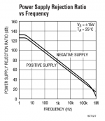
Now if you suppose that the noise in the amplifier subsystem arises from less than infinite power supply rejection, and if we can focus on the first stage and neglect the second, then it seems the gain from input to output is equal to the gain from the power supply to output. Each of them creates 16mV of fuzz at the amplifier output But the forward path gain is +32dB while the opamp PSRR is (-50dB) or lower if I'm reading the datasheet correctly, figure below.
I may not understand your hypothesis properly.
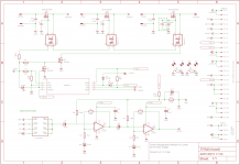
ON THE OTHER HAND there is something on your schematic which worries me. I know this is EagleCAD, but on the schematic system I use ("KiCad") the little crossing at A is a legitimate error. On KiCad, the lack of a big fat solder-dot at A indicates that at least one of (C7, R8, OA1) is not connected to the others. And on KiCad, this is not an ERC error (!!). The only way you'll find it is to look at the ASCII netlist and see an unfamiliar and anonymous nodename. Ever since this happened to me, and I lost 3 weeks because of an extra PCB spin, I have always made an effort to name every net. Now if a netlist shows up as "N0001" it is an immediate red flag.
You want the very same thing at B that you want at A. But EagleCAD has drawn them differently. This should be investigated. You want the same thing at C that you want at A. But EagleCAD has drawn them differently. And what about D? Is that a jumper of two unrelated nets, or is it a 4-way connection that omits the solder-dot, as in A?
Yikes, I'm nervous. Suggest you take out a bare PCB and buzz it with your ohmmeter.
- 0 mV on GND
- 0 mV on 12V
- 0 mV on 3V3
- 16 mV on 5V
- 16 mV self-generated noise in amplifier subsystem
Now if you suppose that the noise in the amplifier subsystem arises from less than infinite power supply rejection, and if we can focus on the first stage and neglect the second, then it seems the gain from input to output is equal to the gain from the power supply to output. Each of them creates 16mV of fuzz at the amplifier output But the forward path gain is +32dB while the opamp PSRR is (-50dB) or lower if I'm reading the datasheet correctly, figure below.
I may not understand your hypothesis properly.
ON THE OTHER HAND there is something on your schematic which worries me. I know this is EagleCAD, but on the schematic system I use ("KiCad") the little crossing at A is a legitimate error. On KiCad, the lack of a big fat solder-dot at A indicates that at least one of (C7, R8, OA1) is not connected to the others. And on KiCad, this is not an ERC error (!!). The only way you'll find it is to look at the ASCII netlist and see an unfamiliar and anonymous nodename. Ever since this happened to me, and I lost 3 weeks because of an extra PCB spin, I have always made an effort to name every net. Now if a netlist shows up as "N0001" it is an immediate red flag.
You want the very same thing at B that you want at A. But EagleCAD has drawn them differently. This should be investigated. You want the same thing at C that you want at A. But EagleCAD has drawn them differently. And what about D? Is that a jumper of two unrelated nets, or is it a 4-way connection that omits the solder-dot, as in A?
Yikes, I'm nervous. Suggest you take out a bare PCB and buzz it with your ohmmeter.
Attachments
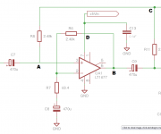
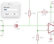
Re the schematic, you are right that it is ambiguous and that there should be a 'junction dot' at A. However, I believe that (luckily) the board itself is correct. See attached images showing the relevant nets, plus an image of the board from Eagle. I have continuity tested the board and it is in accordance with the exported image. (I think in Eagle the over-riding factor is the way the net wires are drawn. Stop/click at another net and a junction is formed. Pass over another net without stopping and no junction is formed. The junction dot is for clarity and, like elsewhere, I should have placed one at A also.)
(B, D and C are as one would expect - no junction dot = no connection and vice versa.)
The 5V and 3V3 regulators are identical except for the 'upper' resistor in the voltage divider of the feedback loop. (Of course, there's part to part variance but the boards and components and their nominal values are identical except for this resistor. 316R for the 3V3 and 1K for the 5V; the 'lower' resistor in the voltage divider being 1K in both.) I'm puzzled as to why the noise measured at the output of the amplifier should be so materially different as when measured elsewhere, un-amplified, both the 5V and 3V3 voltages read about the same. I agree that I don't have a good hypothesis as to why this might come about. I will give it some more thought tomorrow.
Hmm... I realise now that the feed into the amplifier requires the pass transistor switches to be "on". (See the traces into the right side of the dipswitch. I am unsure this was so in which case the readings are horse manure - there should be no voltage on any of them. But it is even more odd in that case that the reading would alter with changes in the dipswitch. Perhaps I am just going mad. I will look again in the morning...
Attachments

Yes the C7 - R8 - OA1pin3 trace is shown in red and it does appear correct. It sounds like EagleCAD's bug is much less pernicious than KiCad's bug. Congratulations!
Coming back to these Vrms and Vpp measurements. When I went to do them properly - with the TPS3510 turning on the pass transistors - I noticed the TPS3510 wasn't working properly. I replaced it. Seems to work fine again.
Measurements of Vpp and Vrms at the amplifier output are much more consistent. While the numbers bounce around a lot on my scope here's the rough output:
GND Vrms ~ 18mV Vpp ~ 40-60mV (flicking between the two)
12V Vrms ~ 21mV Vpp ~ 60-80mV
5V Vrms ~ 21mV Vpp ~ 60-80mV
3V3 Vrms ~ 18mV Vpp ~ 60mV
Also a firmware upgrade to my scope now allows me to save MATH (e.g. FFT) output as a Reference so I will go back to looking at that. Unfortunately I can't see a way to have the frequency scale logarithmic. I'm a long way from being able to present the FFT output in a manner similar to how DIYAudio member preamp did here.
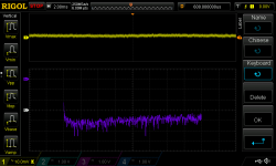
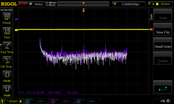
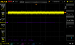
Here are two FFT plots from my scope measuring the 12V. The probe was set to AC coupling and bandwidth limited to 20MHz. I used 'High Resolution'. The FFT window was Rectangle. Vertical axis is 20dB per division with a 60dB offset. For the first pic, I used 2.5kHz per division and so a range from 0-20kHz with 10kHz in the middle. For the second, I used 50Hz per division and so a range from 0-400Hz with 200Hz in the middle. In each case I measured GND and set that as the reference (white).
How do I interpret these in the context of a signal that's been amplified approximately 49dB?
EDIT: these were without a load attached
How do I interpret these in the context of a signal that's been amplified approximately 49dB?
EDIT: these were without a load attached
Attachments

Last edited:
DIYAudio member preamp says
I haven't used the FFT feature of a Rigol scope either, so I can't offer any words of advice.
When I look at your second plot, I notice that
I have no intuition about, and no comment upon, your first plot.
The measurements were performed using ARTA and my ESI Juli@ via ASIO for 24bit resolution. Spectrum data was averaged over 32 runs (totaling about 90 seconds for each circuit) and converted to the LTspice-RAW-format. Graphs were created via LTspice Waveform Viewer using the same scale for each measurement.
I haven't used the FFT feature of a Rigol scope either, so I can't offer any words of advice.
When I look at your second plot, I notice that
- The white GND trace seems not to have peaks at 100 Hz or its harmonics. This suggests (?) that your measurement apparatus does a good job of rejecting mains hum; the final displayed output is free of mains hum artifacts.
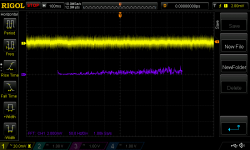
- The purple 12V trace seems to have a peak about 20dB above the noise floor, at 100 Hz. I think this might be surprisingly large; either you've got an incredibly low noise floor, or your regulator has a not-very-good line rejection at 100Hz, or your setup has a terrible hum pickup on the wiring pathway between the 12V regulator and the preamp, or perhaps some of each. It would be good to figure out how to convert these readings to millivolts of amplitude. Maybe they are all subtle shades of "excellent".
- 12V also has similarly tall peaks at 200Hz and 300Hz, which seems fishy to me. I would expect the filter caps to attenuate 200 Hz hum better than they attenuate 100 Hz hum, and 300 Hz better still. Maybe this points to some sort of instrumentation weakness.
I have no intuition about, and no comment upon, your first plot.
It would be good to figure out how to convert these readings to millivolts of amplitude. Maybe they are all subtle shades of "excellent".
It would be nice to think so.
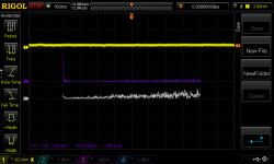
The scope FFT can switch between dB and Vrms. However, the resolution with the latter is too high. The minimum vertical division I could dial in was 200mV per division. (It seems a bit buggy as at one point I couldn't seem to dial in less than 5V and at another I swear I could dial in 100mV. Perhaps the user is buggy. I will keep playing with it.)
Here's a pic. 200Hz in the middle, 50Hz per horizontal division. (Other settings as above.) The FFT info (12V rail) is indistinguishable from the grid.
Attachments
Last edited:
This is better. It's weird - I hit Reset Scale and it allowed me to dial down to 2mV per vertical division. Go figure. And the documentation sucks.
This without rerunning the capture just changing the resolution of the previous image.
0-400Hz at 50Hz per division (2mV vertical). At least we can see some data. Whether to trust it or not is another thing.
EDIT: second pic with noise floor. White is output above, offset -2mV. Purple is noise floor (GND).
Attachments
Last edited:
Wish I knew about this feature of this scope but I do not. Sorry.
What do you think of the idea of using a 9v-battery-powered Quasimodo board as a calibration oscillator? You could connect a 1000-to-1 attenuator to its output, maybe 10K_top, 10R_bottom, and use that to inject a tiny signal of known amplitude and known frequency, into the PSU analyzer preamp. When you make an FFT you would at least know what this one amplitude "should" be, and thereby calibrate the rest of the FFT plot.
Beware, Quasimodo's output has a 4.7K pullup and an 0.006R pulldown. So your attenuator will load it down somewhat. Best thing to do is use your scope to measure the output with the 1000-to-1 attenuator connected, and then just trust the resistor manufacturer to create an accurate 1000-to-1 attenuation.
And maybe it's time to consider buying a signal generator? Mine cost 200USD.
- Status
- Not open for further replies.
- Home
- Amplifiers
- Power Supplies
- Enough current to turn on 3 mosfets?