ok.
so, what do you think about this layout?
If Q1 and Q2 are input transistors they are on the wrong side of the board. The input section should be opposite the power section. VAS is more immune to noise so it should be there.
If that is what you think then I have explained/described it badly.This sounds like an excellent way to induce a lot of noise into a ground.
If Q1 and Q2 are input transistors they are on the wrong side of the board. The input section should be opposite the power section. VAS is more immune to noise so it should be there.
yes Q1/Q2 are input transistor. but this is Elliot layout, have a look:
An externally hosted image should be here but it was not working when we last tested it.
If that is what you think then I have explained/described it badly.
Yes you are explaining things unclearly. The way you first explained it would imply that the ground should run along side the power rail traces. This would make for a noisy ground.
the changing current flowing around a loop creates EMI.
Are you agreed?
The Power supply to the amp board runs in a twisted triplet.
Do you agree the efficacy of this arrangement?
The purpose of the twisted triplet is to maintain a very close coupling of the Flow and Return conductors in the connection.
Are you agreed?
When the power feed arrives at the amp PCB, the same low loop area rules should be complied with.
Are you agreed?
How do you propose to run the +ve power and it's Return and comply with the low loop area rules?
Similarly how do you propose to run the -ve power and it's Return and comply with the low loop area rules?
These three traces/conductor must be run as close coupled to minimise the loop area and minimise the interference emitted by the changing currents in the conductors.
Once you have the three close coupled conductors on the PCB feeding the power devices, you can then add on the HF and MF supply rail decoupling.
These should all meet at a point (or small area) between the power devices.
You need to bring the Output Zobel to this low impedance point.
That small area/point becomes the reference for all other parts of the circuit. This is where you could connect the link to reference the input signal Return. It is the quietest point on the PCB. There should be no long lengths of resistive trace separating all the tappings into that small area. This part of the layout design determines the layout of the whole amplifier.
Are you agreed?
The Power supply to the amp board runs in a twisted triplet.
Do you agree the efficacy of this arrangement?
The purpose of the twisted triplet is to maintain a very close coupling of the Flow and Return conductors in the connection.
Are you agreed?
When the power feed arrives at the amp PCB, the same low loop area rules should be complied with.
Are you agreed?
How do you propose to run the +ve power and it's Return and comply with the low loop area rules?
Similarly how do you propose to run the -ve power and it's Return and comply with the low loop area rules?
These three traces/conductor must be run as close coupled to minimise the loop area and minimise the interference emitted by the changing currents in the conductors.
Once you have the three close coupled conductors on the PCB feeding the power devices, you can then add on the HF and MF supply rail decoupling.
These should all meet at a point (or small area) between the power devices.
You need to bring the Output Zobel to this low impedance point.
That small area/point becomes the reference for all other parts of the circuit. This is where you could connect the link to reference the input signal Return. It is the quietest point on the PCB. There should be no long lengths of resistive trace separating all the tappings into that small area. This part of the layout design determines the layout of the whole amplifier.
Last edited:
yes Q1/Q2 are input transistor. but this is Elliot layout, have a look:
An externally hosted image should be here but it was not working when we last tested it.
Now that you've added a picture to match the board design I see a whole lot more I don't like. The output connection shouldn't be anywhere near the input connection. The two most sensitive transistor connections in just about every amplifier are the base pins on the input transistor and the feedback transistor. These should be as far away as possible from high current, both on the board as well as in the chassis.
I agree with you up until the power enters the amplifier board. After the rail caps on the power connectors there is nothing to filter noise from the rails or ground. I try to run the speaker output traces along the power rails to reduce EMI on the board. Current is flowing equally in opposite directions in both those traces which should have a better cancelling effect than the ground would. I also plan the chassis before hand so there won't be any sensitive circuitry or wiring in that area anyways. Other than my first Slewmaster amp, every amp I've built has been absolutely silent without any fuss when installed in chassis so I must be doing something right.the changing current flowing around a loop creates EMI.
Are you agreed?
The Power supply to the amp board runs in a twisted triplet.
Do you agree the efficacy of this arrangement?
The purpose of the twisted triplet is to maintain a very close coupling of the Flow and Return conductors in the connection.
Are you agreed?
When the power feed arrives at the amp PCB, the same low loop area rules should be complied with.
Are you agreed?
How do you propose to run the +ve power and it's Return and comply with the low loop area rules?
Similarly how do you propose to run the -ve power and it's Return and comply with the low loop area rules?
These three traces/conductor must be run as close coupled to minimise the loop area and minimise the interference emitted by the changing currents in the conductors.
Once you have the three close coupled conductors on the PCB feeding the power devices, you can then add on the HF and MF supply rail decoupling.
These should all meet at a point (or small area) between the power devices.
You need to bring the Output Zobel to this low impedance point.
That small area/point becomes the reference for all other parts of the circuit. This is where you could connect the link to reference the input signal Return. It is the quietest point on the PCB.
It was the quietest point until you connected the Zobel to it. The Zobel output is filthy. It shouldn't connect to the same point as the input section.
This is the description of the Flow and Return pair.I agree with you up until the power enters the amplifier board. After the rail caps on the power connectors there is nothing to filter noise from the rails or ground. I try to run the speaker output traces along the power rails to reduce EMI on the board. Current is flowing equally in opposite directions in both those traces which should have a better cancelling effect than the ground would.
I also plan the chassis before hand so there won't be any sensitive circuitry or wiring in that area anyways. Other than my first Slewmaster amp, every amp I've built has been absolutely silent without any fuss when installed in chassis so I must be doing something right.
The Output Zobel must return to the HF decoupling. That is the lowest impedance point for the above audio frequencies. From output device to Zobel back through the HF decoupling and into the output device is the current loop. It's that loop that must be compact and short to allow the HF to flow with least impedance.It was the quietest point until you connected the Zobel to it. The Zobel output is filthy. It shouldn't connect to the same point as the input section.
Current flowing in longer traces will create excessive volts drops and that will create avoidable noise.
The input section is completely separate.
The Output Zobel must return to the HF decoupling. That is the lowest impedance point for the above audio frequencies. From output device to Zobel back through the HF decoupling and into the output device is the current loop. It's that loop that must be compact and short to allow the HF to flow with least impedance.
Current flowing in longer traces will create excessive volts drops and that will create avoidable noise.
The input section is completely separate.
And where does the input ground connect to in your layout?
Very interesting debate. I follow with interest.
But would someone draw an "universal" layout?
A simple schematic, maybe also made by a pencil 🙂
It will be verh helpfull dor many people here on the forum
But would someone draw an "universal" layout?
A simple schematic, maybe also made by a pencil 🙂
It will be verh helpfull dor many people here on the forum
Very interesting debate. I follow with interest.
But would someone draw an "universal" layout?
A simple schematic, maybe also made by a pencil 🙂
It will be verh helpfull dor many people here on the forum
This is tough to draw. A diagram would no sooner be posted and 5 others would pipe up and say it's wrong but not actually say why or what would be better.
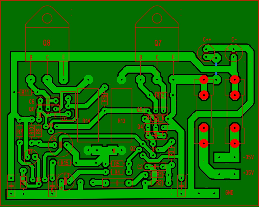
Here's an example of an output stage layout. As always it's not ideal. This time it's due to size constraints. High power traces and the ground connection to the supply inlet caps would be changed to planes at the end of the layout process but it'll give you the main idea. Power rail connections go to the supply inlet capacitors. Current follow a distinct separate path out of those capacitors to the output devices. The separate path is important. Ground to the input stage comes from a star point on the inlet side of the supply caps. Zobel ground on the opposite side of the caps. The Zobel dumps a lot of high frequency garbage to ground so I prefer to connect it right at the inlet ceramic/film input caps to allow them to dump this noise into the power rails away from the sensitive input ground. The VAS section would be next on the left side of the board with the input at the far left, as far away as reasonably possible from the high current areas.
Attachments

- Status
- Not open for further replies.
- Home
- Amplifiers
- Solid State
- Dx Blame ST - Builder's thread - post pictures, reviews and comments here please.