What?Sorry Alex...I was only trying to help the community since ostripper is nowhere to be seen but seems Andrew knows what to do.
Again.
Can anyone reverse engineer the Gerber files back to a PCB layout in it's various layers?
I see you too were asking for help...
but you were quite rude to Alex...need some manners around here.
I was not being rude to Alex.
I never mentioned Alex nor the fact he volunteered to take on a redesign of the PCB layout.
I was referring to all you i****s that were asking a for a redesign when OST has already designed the PCB layout for us.
I never mentioned Alex nor the fact he volunteered to take on a redesign of the PCB layout.
I was referring to all you i****s that were asking a for a redesign when OST has already designed the PCB layout for us.
I did not ask Alex for a redesign, only for help
Andrew be a man and say what you need to say with all it letters... don't use *** that many don't understand.
Andrew be a man and say what you need to say with all it letters... don't use *** that many don't understand.
Hi,
Just my opinion as I like OS creations.
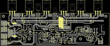
OS layout as it developed turned out to be a good one, much better than the 'schematic style' PCB's that's so common. I like OS layout as current loop areas are outside of small signal areas etc. Of course it could be even better but that would probably mean more layers and that may not be desirable.
I think the best way to honor OS is to make a PCB in a style OS had in mind.
Just my opinion as I like OS creations.
OS layout as it developed turned out to be a good one, much better than the 'schematic style' PCB's that's so common. I like OS layout as current loop areas are outside of small signal areas etc. Of course it could be even better but that would probably mean more layers and that may not be desirable.
I think the best way to honor OS is to make a PCB in a style OS had in mind.
 AndrewT, You should calm down. Please stop insulting people.
You made some statements which may not be correct. Yes it was planned for ostripper to be gone for a while, but he returned, we exchange some posts and e-mails, he did an update, but then he disappeared again, and won't answer e-mails PM's or posts. While we are concerned that he is having problems of some sort, we can't wait forever, and it is looking like forever at this point.
Also, the suggestion was that Alex recreate the ostripper schematic, NOT redesign it, so you are incorrect there too. And Alex, we appreciate your offer, which wasn't in fact even your idea!
However, it is a step backwards to redo something that we have built an etched prototype for using ostripper boards, and has been proven to work, We'll review the files one more time to made sure the mounting holes are wrong. If they are we will then we'll decide whether to order anyway or not. To most people , the incorrect mounting holes is not a big deal, but we we're hoping the create this standard,, as in the long run, it will be VERY helpful, if all orr boards adhere to it..
It would be useful if someone know how to edit a Gerber file, if that's possible (we think it isn't but there are lots of clever people and programs out there.. )
Last edited:
I second using OS's own PCB layout. Can someone make a post with all the relevant images/files up to this point?
Ehhm, I did a quick browse, but I can't find any gerber files in any of the .zips in this thread. If anyone has them please PM me.
If no gerber files surface I'll have to redraw the whole thing from scratch. Don't worry though I will follow OS's design as faithfully as I can. My component library only have round pads so polygon ones might take a while since I have to change them by hand. Won't be too hard given how altium is pure awesome, but I'll start with round/oval ones.
And in case you're wondering, I have plenty of layout experience so hopefully I won't disappoint you. I'll start tomorrow if no gerber files show up in the meantime.
Yes... from post 188?
No, from OS's web site.
Regards,
currentflow
Just checked this and no it wasn`t from post #188, this file doesn`t include Gerber`s at all.Yes... from post 188?
Must have been from OS`s website (later) .
See, knew I missed something.
I've loaded up the files and from what I can see the distances between the output devices (c-c) are all 40mm (that's what people worried about if I understand correct). Hard to measure with any insane accuracy since there's no snap function or anything. Anything else that needs measuring?
Will do more tomorrow afternoon, now I need sleep.
PM sent to Mjjg. Please don't post links to possible Gerber's here. We need to work with the latest files , and we'd also prefer not to have these show up on e-bay after we've invested in hiring ostripper. Especially since the potential e-bay versions may be the wrong version. But, in exchange, we'll stop hoping for os to respond, and move forward on the small corrections needed, or if that doesn't work out, send them out as they are, as its mostly the mounting holes that are the problem..
Once the boards are in production, and some built, we'll post the Gerbers
Mark
Once the boards are in production, and some built, we'll post the Gerbers
Mark
Last edited:
Cannot believe You knocked this up during the short time since Your last post only a couple of hours before 😱 or did You work on this already before?........ I can generate Gerber's for OS PCB just let me know . 😉
I cant let you down diy guys 🙂 It was first step .......
Alex.
This is a great project. There are probably a few willing to redraw the PCB from scratch following OS's layout, if required. It would be regrettable to have OS out of the loop though.
Whoa....this thread came alive...
If my post was not clear.... I do agree that any new pcb layout has to follow OS's layout as close as possible - only deviating to accomodate the diyAudio mounting standard.
Any and all credit should also stay with OS.
I think that Alex worked with ostrippper to create the first version. Maybe the best thing is to send the latest version to Alex and he (and I ) check for changes and update the board. Then he can move the holes around as we wish, and we're good to go!!
Os version that I made was shown in post 170.
http://www.diyaudio.com/forums/solid-state/192431-class-ab-amp-diyaudio-17.html#post2648822
There was nothing wrong with the layout that OS produced. It works, and quite well I must say. Maybe it could have been a little more compact as it is fairly large, but that is all.
Regards
Simon
http://www.diyaudio.com/forums/solid-state/192431-class-ab-amp-diyaudio-17.html#post2648822
There was nothing wrong with the layout that OS produced. It works, and quite well I must say. Maybe it could have been a little more compact as it is fairly large, but that is all.
Regards
Simon
Attachments

Looking at niss_man photos I would suggest we need a right hand side and a left hand side board for proper layout in the case.
Power side to the front of the box and input to the rear
Power side to the front of the box and input to the rear
Last edited:
Looking at niss_man photos I would suggest we need a right hand side and a left hand side board for proper layout in the case.
Power side to the front of the box and input to the rear
I wouldn't bother. It works well with zero noise already.
- Home
- Amplifiers
- Solid State
- diyAB Amp - The "Honey Badger"