in one of Nelson Pass's online lectures, he said he has grown tired of pencil calculations, so now he used pots to find optimum values of resistors in his circuits and then replace the pots with nearest standard value resistors....once resistors are known, any capacitors needed is easy to know using online rc calculators...
I was looking for the reason why the TTA/TTC004B base currents spike at high output voltage. Looking at the SPICE models, we see:
TTC004B:
Vaf=11.95
Var=1000
TTA004B:
Vaf=6.8
Var=50
Well those are suspiciously low values for forward Early voltage and suspiciously high values for reverse Early voltage. What do you want to bet they got the forward and reverse parameters swapped when doing measurements? The datasheets do not show such awful Early voltage.
I wonder if we can expect any other parameters to be screwed up? I'm eyeing RE/RC in the TTA004B model.
I have noticed on Badger V2 , the cascode in the design seems to not only clip
perfectly , but the diode type (model) does not add THD short of clipping ?
Any diode - no difference. Higher Z of the cascode ? ... All I know is
the clipping response is symmetrical and perfect. Perhaps KT can shed
light on why ???
PS - I was about to get anal with an active clamp - the single diode (D3)
exceeded expectations. :🙂
OS
OS
Referencing schematic on post #2319, Try deleting C7 and D3 and check clipping behavior.
Here are some models that modify the existing models:
.model TTC004B_ex AKO:TTC004B_BJT VAF=1000 VAR=11.95
.model TTA004B_ex AKO:TTA004B_BJT VAF=50 VAR=6.8 RB=1
Paste this onto your schematic and rename your BJTs to TTC004B_k and TTA004B_k. Ostripper's models must already be present for this to work.
Base current will increase but will be less spiky. Early voltage is the voltage at which Hfe doubles so a low Early voltage means that at high voltages the Hfe will increase. For instance a VAF of 6.8 means that at 68V your Hfe will increase by 10 times! Totally unrealistic for a medium power high voltage BJT.
Referencing schematic on post #2319, Try deleting C7 and D3 and check clipping behavior.
Yes, this uses the buffer C-B junction as a clamping diode that activates when the buffer current gets too high. The resistor used to be 220 ohms which limited the current to about 200mA.
OS
Referencing schematic on post #2319, Try deleting C7 and D3 and check clipping behavior.
Tried it. Q13 collector rings like hell. But you saw the output look "not so bad".
Add C7 , Q13 collector stops ringing , but output looks bad.
Add D3 , both Q13 (current) and the output look VERY good.
Q13 never passes more than 2ma , even D3 never clamps more than 3ma.
Lower R17 >1K , like Badger V1 .... Clamp is essential to keep Q13 collector
current safe. On the current Badger , the clamp can pass 10-20ma - as can
Q13 without a clamp. Poor Q13 😀 .
It seems C7/D3 are a happy medium for the (safer) high(er) impedance Q13
collector.
Edit another benefit of R17/C7 is a nice stable voltage of 1/2 the negative rail
so I can use the BC550.
OS
Last edited:
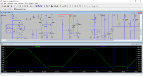
Here is the ac response R17=22k C7=not installed, D3=not installed but I had to disable the DC servo. R17=22k might not be the most optimum value, the value of R17 using this method needs to be 10 to 20 times greater than R19. I don't have have an issue with D3 being installed I was suggesting an alternative means. D3 would have to have low leakage current over a large voltage swing to keep distortion low.
Attachments

Q13 is back to a 1845 , and we lose the diode and C7.
Why not just get rid of everything and hook Q13's collector to the
base of Q12 ? Get to keep the BC , as well.
- get to keep the BC.
-LED's would flash on clip.
-NO diode
-4 ppm @ 20khz ... cool.
OS
Why not just get rid of everything and hook Q13's collector to the
base of Q12 ? Get to keep the BC , as well.
- get to keep the BC.
-LED's would flash on clip.
-NO diode
-4 ppm @ 20khz ... cool.
OS
Last edited:
Yep, that's another way of doing it. In that case you get something like a 2-stage clamp, where the cascode transistor saturates first and then the buffer saturates. This means that the buffer collector is protected from voltage swing up until just before clipping, and so the leakage/capacitance of your diode or B-C junction no longer matters for performance under normal conditions.
The tradeoff is that you lose some Hfe in the buffer transistor because the collector voltage is lower. If your Early voltage is 60V for instance, then at 60Vce you will get double the Hfe in the buffer transistor.
The tradeoff is that you lose some Hfe in the buffer transistor because the collector voltage is lower. If your Early voltage is 60V for instance, then at 60Vce you will get double the Hfe in the buffer transistor.
Q13 is back to a 1845 , and we lose the diode and C7.
Why not just get rid of everything and hook Q13's collector to the
base of Q12 ? Get to keep the BC , as well.
- get to keep the BC.
-LED's would flash on clip.
-NO diode
-4 ppm @ 20khz ... cool.
OS
I like that idea and you could go back to the BC546 because the LED will keep VCE low.
Self clamping is neat.The Hawksford symmetrical also does this.
Also - gained many db of PSRR at LF , the VAS is no longer ground
referenced.
OS
Also - gained many db of PSRR at LF , the VAS is no longer ground
referenced.
OS
Last edited:
I wonder if you could add another LED between R18 and the base of Q12 and tie the collector of Q13 to the top or anode of the added LED to get the collector voltage up.
Just for interest's sake.
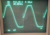
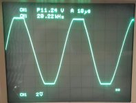
Here is a waveform at 110Vp-p of an ef follower VAS "not cascoded". During Clipping. And how it looked after adding a clamping diode.
I did further work on the design but don't remember everything I did back then.
Regards
Here is a waveform at 110Vp-p of an ef follower VAS "not cascoded". During Clipping. And how it looked after adding a clamping diode.
I did further work on the design but don't remember everything I did back then.
Regards
Attachments
That looks great OS! A much better solution. I'll check the sim again after some sleep. I think I might like to have a jumper option to add the cap in series with R9 in case you don't want to use the DC servo.
- Home
- Amplifiers
- Solid State
- diyAB Amp - The "Honey Badger"