Ok. Got sidetracked.
I read the instructions of how to set things up to test up to the output stage. Specifically:
"DO NOT solder in R36.
Instead temporarily solder 2- 68R resistors between R40 and R37 and the long output trace that is hooked to L1. This will turn your drivers into the outputs !
When powering up for the first time either use the 2 fuse safety resistors (R53 and 54) , or solder 2 "sacrificial" 10R 1/4-1/2W resistors to the "V+ and V-"
terminals (after the fuses)."
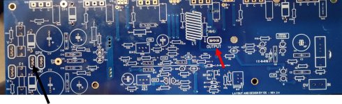
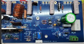
See photos of board with R53 and R54 in place. And R36 removed. But I'm not clear on how to install 68R resistors from R40 to R37 to long output trace to L1. I've drawn what I think I'm supposed to do. Appreciate further insight.
I read the instructions of how to set things up to test up to the output stage. Specifically:
"DO NOT solder in R36.
Instead temporarily solder 2- 68R resistors between R40 and R37 and the long output trace that is hooked to L1. This will turn your drivers into the outputs !
When powering up for the first time either use the 2 fuse safety resistors (R53 and 54) , or solder 2 "sacrificial" 10R 1/4-1/2W resistors to the "V+ and V-"
terminals (after the fuses)."
See photos of board with R53 and R54 in place. And R36 removed. But I'm not clear on how to install 68R resistors from R40 to R37 to long output trace to L1. I've drawn what I think I'm supposed to do. Appreciate further insight.
Attachments
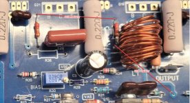
Connect R40 to the output trace and R37 to the output trace. To make it really easy, just connect a 68 ohm resistor from base to emitter pads on Q18 and Q21. That's basically the same thing.
I'm not trying to be critical, but your output inductor looks pretty rough. It needs to be fairly neatly wound to operate correctly, These are kind of tough to figure out how to do but with a little practice they're actually quite easy to wind.
I'm not trying to be critical, but your output inductor looks pretty rough. It needs to be fairly neatly wound to operate correctly, These are kind of tough to figure out how to do but with a little practice they're actually quite easy to wind.
Well, can't believe it but I finally powered up the right channel for the HB.
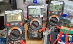
Both LEDs turned on. Check.
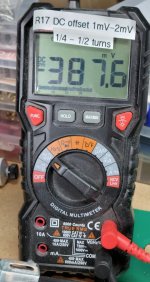
R7 showed 0V. Check
But R17 quickly ran up to -387.6 mV. I turned the amp off to reflect.
The R17 reading doesn't look right. I have set the R17 for a middle position per the guide.
I'm connecting the positive to the speaker output and the negative terminal to ground as shown.
With a reading as shown above [and it was still climbing when I turned the amp off], seems like I've missed something?
Thanks
Both LEDs turned on. Check.
R7 showed 0V. Check
But R17 quickly ran up to -387.6 mV. I turned the amp off to reflect.
The R17 reading doesn't look right. I have set the R17 for a middle position per the guide.
I'm connecting the positive to the speaker output and the negative terminal to ground as shown.
With a reading as shown above [and it was still climbing when I turned the amp off], seems like I've missed something?
Thanks
Attachments
It looks like your amp is working correctly, otherwise the output would head for one of the rail voltages. 380mV is nothing to worry about. You need to adjust R7 so you have the correct current flow through the input stage. I think the recommended current was 3.5mA. You measure the voltage drop across R14 to calculate this current.
You need to adjust R17 to zero out the DC offset at the output, but the input stage current needs to be flowing properly for this.
You need to adjust R17 to zero out the DC offset at the output, but the input stage current needs to be flowing properly for this.
Correct me if I'm wrong, you also should NOT have the speaker hooked up while adjusting the input stage current, DC offset and bias.

So you are saying I should move the R7 leads from the R53 resistor to the R14 resistor to adjust the trim pot to around 3.5mA. But how do I set the DMM to read across R14? I'm missing something here.It looks like your amp is working correctly, otherwise the output would head for one of the rail voltages. 380mV is nothing to worry about. You need to adjust R7 so you have the correct current flow through the input stage. I think the recommended current was 3.5mA. You measure the voltage drop across R14 to calculate this current.
You need to adjust R17 to zero out the DC offset at the output, but the input stage current needs to be flowing properly for this.
Set the meter to measure volts. You calculate the current using ohms law. The schematic says R14 should be passing 3.75mA. .00375A x 2200 ohms = 8.25V.
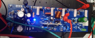
Saw smoke after 30-60 seconds with the power on.
R25 went up in smoke as I was getting ready to start the bias process.
The DBT was in the circuit and didn't reveal a short.
I was getting a reading on the R7 DMM indicating current.
I have set this up to bias without the output stages in place.
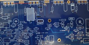
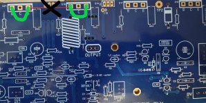
I removed R36. And you can see the red connectors on Q18 and Q21.
I have 10W resistors in place of fuse for R53+R54.
I don't see any other burn victims.
I have replaced the R25 [220R] but would appreciate any thoughts before I try again.
And thanks.
R25 went up in smoke as I was getting ready to start the bias process.
The DBT was in the circuit and didn't reveal a short.
I was getting a reading on the R7 DMM indicating current.
I have set this up to bias without the output stages in place.
I removed R36. And you can see the red connectors on Q18 and Q21.
I have 10W resistors in place of fuse for R53+R54.
I don't see any other burn victims.
I have replaced the R25 [220R] but would appreciate any thoughts before I try again.
And thanks.
Attachments

Q9 must be passing too much current to make R25 burn. Either it's incorrect or there is issues in the input stage drawing too much current from it's base.
I recall someone else having the same problem recently. Might be worth reviewing both the Honeybadger threads to see what their issue was.
I recall someone else having the same problem recently. Might be worth reviewing both the Honeybadger threads to see what their issue was.
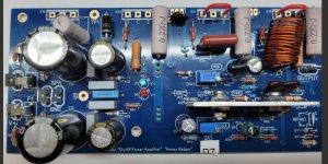
I didn't look too close at the pictures. Those red jumper wires should be 100 ohm resistors. You also need to install the drivers and bias spreader transistor.
1. I will replace jumpers with 100 ohm resistors
2. Which drivers do I need to install?
3. What is the bias spreader transistor? a search of this forum brings up:
I am of the understanding that in this method the vbe multiplier transistor should NOT be mounted on the heatsink as it should have nothing to do with thermal bias, so i am thinking that it was a error of the silicon chip design to mount the bd139 on the heatsink.
Bob Cordell talks about this a lot in his book designing audio power amplifiers. I have copied the image below from his book, i hope he does not mind it as it is to show the method."
This is way above my pay grade.
I'm following C. in the options.txt notes in order to bias everything up to the output stage devices. Perhaps I've lost the thread and I should install all the output stage transistors and bias from that state.
2. Which drivers do I need to install?
3. What is the bias spreader transistor? a search of this forum brings up:
Yes, they are the NJL3281 thermal track devices. The thermal track transistors diodes by themselves alone proved inadequate for thermal bias stability despite the datasheet claims, therefore it is necessary to use them together with a traditional vbe multiplier (bias spreader) to achieve thermal stability. They are generally placed in series with the traditional vbe multiplier. The tracking diodes introduce the temperature effects of the output transistors, while the vbe multiplier transistor takes care of controlling that part of the bias spread necessary for the predriver and driver transistors.I see 5 pin power devices. What are these? Do they contain temperature sensing diodes (ThermalTracks)? If so, why's there also this BD139 Vbe multiplier?
Best regards!
I am of the understanding that in this method the vbe multiplier transistor should NOT be mounted on the heatsink as it should have nothing to do with thermal bias, so i am thinking that it was a error of the silicon chip design to mount the bd139 on the heatsink.
Bob Cordell talks about this a lot in his book designing audio power amplifiers. I have copied the image below from his book, i hope he does not mind it as it is to show the method."
This is way above my pay grade.
I'm following C. in the options.txt notes in order to bias everything up to the output stage devices. Perhaps I've lost the thread and I should install all the output stage transistors and bias from that state.
Drivers are Q14 and Q15.
Bias spreader is Q13.
It's advisable that you follow the known path and stay away from modifications from which you do not completely understand the consequences.
Bias spreader is Q13.
It's advisable that you follow the known path and stay away from modifications from which you do not completely understand the consequences.
Dave, I've searched too on the question of mica + paste vs. keratherm, and not quite certain the answer. I've searched photos as well. Can you comment on in which direction you went?Hi Folks,
Quick question regarding insulators on the larger transistors. I see in the build guide that mica insulators with thermal paste are recommended. Would a thermal pad such as the Keratherm pad work also? I'm putting together another parts order and wondering if the mica/grease combo was recommended for a specific reason.
Thank you in advance. Dave M.
thanks,
Chip
- Home
- Amplifiers
- Solid State
- diyAB Amp The "Honey Badger" build thread