Hi Kay
- R3, R6 = 22 kΩ in the V2.4 schematic vs. R3, R6 = 33 kΩ in the build guide is to reduce the overall amplifier gain from about 40 to 26
...- R24 = 1.5 kΩ in the V2.4 schematic vs. R24 = 820 Ω in the build guide, gain related.
What does "gain related" (R24) mean? How is it related to gain? Is R24 related to R3+R3 (pun intended)? How? If the V2.4 values are used for R3+R6, should R24 also be changed to to the V2.4 values or are they independent?
I know I am repeating myself, but selling the V2.4 board with the outdated build guide is confusing.
I think, as the overall voltage gain is reduced from about 40 to about 26, the value of R24 in the compensation network will have to be adapted, just for performance and stability purposes. Btw, I agree with your complaint on confusion. I'd also prefer a straightforward guideline. Best regards!
Hi Kay
Cheers
- R3, R6 = 22 kΩ in the V2.4 schematic vs. R3, R6 = 33 kΩ in the build guide is to reduce the overall amplifier gain from about 40 to 26
- R23 = 47 Ω in the V2.4 schematic vs. R23 = 33 Ω in the build guide for the higher CCS current
- R24 = 1.5 kΩ in the V2.4 schematic vs. R24 = 820 Ω in the build guide, gain related.
- R26 = 10 Ω in the V2.4 schematic vs. R26 = 100 Ω in the build guide, higher CCS current
- R27 = 82 Ω in the V2.4 schematic vs. R27 = 68 Ω in the build guide, increases the current to about 10mA and helps remove ringing for square wave or clipping
- the "diode fix" (baker clamp or D-BC) also removes output ringing - BAV21
- the LC option - add a 2pF cap across R6 to slightly improve HF response
John
Thanks a lot for your detailled reply, John! The V2.4 schematics designates said D10 »baker clamp« as MMSD4148 - supposedly a SMD derivative of the good old thru-hole 1N4148. As the V2.4 board is already prepared for a leaded component in this place, why should we prefer a BAV21 here? Best regards!
Hi,
are there any objections against substituting the current sensing devices Q8 (KSC1845) and Q11 (2SC3503C) by cheaper TO92 transistors, such as BC550C?
Best regards!
are there any objections against substituting the current sensing devices Q8 (KSC1845) and Q11 (2SC3503C) by cheaper TO92 transistors, such as BC550C?
Best regards!
Do not use 1n4148, too much leakage current and too low PIV. That is a mistake that should be fixed in the schematic.
Only adding D10 fixes the bad behavior at clipping. See post 591 for the explanation of the problem. The rest of the changes are just minor improvements to further reduce distortion near clipping.
One reason the build guide has not been updated, is the staff at DiyAudio store have not had a chance to build the pcb with the latest component values yet. The other reason is that one can still follow the existing build guide to assemble the v2.4 PCB without issue.
One reason the build guide has not been updated, is the staff at DiyAudio store have not had a chance to build the pcb with the latest component values yet.
...and perhaps won't have in any future, as I managed to buy the last available pair?
Thanks for the other hints you gave me, btw

Best regards!
Another question: Is there any template, or a scetch, available for drilling the holes in the heatsinks?
Best regards!
Best regards!
The rest of the changes are just minor improvements to further reduce distortion near clipping.
Does that imply that changing the gain using different values for R3 and R6 is not related to changing the value of R24? In other words: R3+R6 define the gain only (nothing to do with clipping behaviour), and R24 is related to distortion near clipping only (nothing to do with gain)?
amplifier gain is set with R6 & R5. Gain = 1+(R6/R5)
matching of R3 to R6 is to minimise the input voltage offset and thus the output offset.
Don't use the 1k VR17 to change the output offset. Match the LTP operating currents and voltages. Leave VR17 empty.
R24 sets the phase margin of the internal feedback loop.
I can't see a BAV21.
My copy of the sch is dated 7/17/11
Last edited:
I can't see a BAV21.
My copy of the sch is dated 7/17/11
May I say I feel some comfort to see that mbrennwa and me are not the only ones to be confused? Doesn't really help, though.
Best regards!
Sorry for nagging, but I do not fully understand how the modifications of the VAS CCS work:
Should these changes all be applied in combination with each other, correct?
What about changing R12 and R13 to lower values as described here?
Should the R23+R26+R27 change and the R12+R13 change be applied simultaneously? Or just one of the two?
- R23 = 47 Ω in the V2.4 schematic vs. R23 = 33 Ω in the build guide for the higher CCS current
- R26 = 10 Ω in the V2.4 schematic vs. R26 = 100 Ω in the build guide, higher CCS current
- R27 = 82 Ω in the V2.4 schematic vs. R27 = 68 Ω in the build guide, increases the current to about 10mA and helps remove ringing for square wave or clipping
Should these changes all be applied in combination with each other, correct?
What about changing R12 and R13 to lower values as described here?
Should the R23+R26+R27 change and the R12+R13 change be applied simultaneously? Or just one of the two?
Pardon me for nagging, too, but I'd prefer to understand what I'm doing - and to learn - over just cloning.
I must say that mbrennwa's questions are more than just good cause. To my unterstanding at least the current of such a ring-of-two CCS is defined by the sense transistor's Vbe, divided by the value of the sense resistor. Thus - why do we gain a current increase by increasing this resistor?
Best regards!
Another question: Is there any template, or a scetch, available for drilling the holes in the heatsinks?
Best regards!
As mentioned in the build guide, the Honey Badger conforms to the UMS spec at the DiyAudio store.
Universal Mounting Specification – diyAudio Store
amplifier gain is set with R6 & R5. Gain = 1+(R6/R5)
matching of R3 to R6 is to minimise the input voltage offset and thus the output offset.
Don't use the 1k VR17 to change the output offset. Match the LTP operating currents and voltages. Leave VR17 empty.
R24 sets the phase margin of the internal feedback loop.
I can't see a BAV21.
My copy of the sch is dated 7/17/11
While one can omit the the R17 trimmer if the LTP transistors and resistors are perfectly matched, I would prefer to have the trimmer on hand in case of problems.
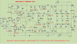
The v2.4 schematic is the green picture on the store page for the PCB.
http://cdn.shopify.com/s/files/1/1006/5046/products/badger_v2.4_1024x1024.gif
As mentioned in the build guide, the Honey Badger conforms to the UMS spec at the DiyAudio store.
Universal Mounting Specification – diyAudio Store
Thanks a lot! I didn't assume yet that informations on the Honey Badger would be distributed to such many sources, even some beyond this board.
Btw, the SS mounting holes are the ones in the lowermost row, right?
Could this drawing, for contrast reasons, be converted into one with just plain white background?The v2.4 schematic is the green picture on the store page for the PCB.
http://cdn.shopify.com/s/files/1/1006/5046/products/badger_v2.4_1024x1024.gif
Best regards!
Last edited:
As mentioned in the build guide, the Honey Badger conforms to the UMS spec at the DiyAudio store.
Universal Mounting Specification – diyAudio Store
While one can omit the the R17 trimmer if the LTP transistors and resistors are perfectly matched, I would prefer to have the trimmer on hand in case of problems.
The v2.4 schematic is the green picture on the store page for the PCB.
http://cdn.shopify.com/s/files/1/1006/5046/products/badger_v2.4_1024x1024.gif
not unbalancing the LTP.matching of R3 to R6 is to minimise the input voltage offset and thus the output offset.
Sorry for nagging, but I do not fully understand how the modifications of the VAS CCS work:
Should these changes all be applied in combination with each other, correct?
What about changing R12 and R13 to lower values as described here?
Should the R23+R26+R27 change and the R12+R13 change be applied simultaneously? Or just one of the two?
- R23 = 47 Ω in the V2.4 schematic vs. R23 = 33 Ω in the build guide for the higher CCS current
- R26 = 10 Ω in the V2.4 schematic vs. R26 = 100 Ω in the build guide, higher CCS current
- R27 = 82 Ω in the V2.4 schematic vs. R27 = 68 Ω in the build guide, increases the current to about 10mA and helps remove ringing for square wave or clipping
Should these changes all be applied in combination with each other, correct?
What about changing R12 and R13 to lower values as described here?
Should the R23+R26+R27 change and the R12+R13 change be applied simultaneously? Or just one of the two?
- R3, R6 = 22 kΩ in the V2.4 schematic vs. R3, R6 = 33 kΩ in the build guide is to reduce the overall amplifier gain from about 40 to 26
- R23 = 47 Ω in the V2.4 schematic vs. R23 = 33 Ω in the build guide for the higher CCS current
- R24 = 1.5 kΩ in the V2.4 schematic vs. R24 = 820 Ω in the build guide, gain related.
- R26 = 10 Ω in the V2.4 schematic vs. R26 = 100 Ω in the build guide, higher CCS current
- R27 = 82 Ω in the V2.4 schematic vs. R27 = 68 Ω in the build guide, increases the current to about 10mA and helps remove ringing for square wave or clipping
- the "diode fix" (baker clamp or D-BC) also removes output ringing - BAV21
- the LC option - add a 2pF cap across R6 to slightly improve HF response
Ok, I built my Honey Badger using the resistor values given in the V2.4 schematic (I attached a copy of this, just in case the one in the diyAudio store gets changed or removed). I can report that the amp works ok using the V2.4 values. The only exception was that the current in the "big" CCS was only 6.7 mA, which is a bit low for the MJE350/340. I therefore lowered the value of R27 from 82 Ω to 53 Ω, and got about 9.8 mA. (This is described here, but is not documented in the V2.4 schematic).
Who's got the source document of the build guide and the schematic? It would be nice to update these files from the "old" version to V2.4.
Attachments
is that -79mV at the LTP bases, or 0.79mV?
15mVre for the outputs is quite low.
Ost may have found this setting actually gave the lowest crossover distortion.
If you push up the bias voltage @ the multiplier, that will increase the driver Vre as well and thus give a higher bias current.
The EF output stage is s little more tolerant of over biasing relative to optimum rather than underbiasing.
On this basis, I would bias higher so that Ost's value of 15mVre is always the worst case lowest bias.
Last edited:
is that -79mV at the LTP bases, or 0.79mV?
I just copied this file from here. I don't know if the (simulated?) voltage values are correct, but I'll measure it in my build.
15mVre for the outputs is quite low.
What does "re" refer to?
Ost may have found this setting actually gave the lowest crossover distortion.
If you push up the bias voltage @ the multiplier, that will increase the driver Vre as well and thus give a higher bias current.
Assuming you are referring to Q13+R28+R29+R30+R31 as the "multiplier", this is exactly how the biasing of the output stage works. R30 is a trimpot (not shown correctly in the schematic), which is used to set the bias.
The EF output stage is s little more tolerant of over biasing relative to optimum rather than underbiasing.
On this basis, I would bias higher so that Ost's value of 15mVre is always the worst case lowest bias.
I believe the 15 mV value is conservative for cool operation (with smallish heatsinks?). I biased mine a bit higher.
is that -79mV at the LTP bases, or 0.79mV?
The voltages I measured in my build are closer to -13 mV.
- Home
- Amplifiers
- Solid State
- diyAB Amp The "Honey Badger" build thread