OK , there is a serious mistake.
- C115/117 reverse polarity.
-R112 needs to connect to V+. Just swap colors on the R112/113 railbound
traces. R112's trace will be green , connect to V+. R113's driver bound trace
will be blue ... might have to adjust creep relative to V-.
At present R112/113 are both powered by V-.
Edit - creep between R113/driver can be small V- = -60V and Driver collector
-58.5V .. just a 1.5V max difference.
OS
Last edited:
OK , there is a serious mistake.
- C115/117 reverse polarity.
-R112 needs to connect to V+. Just swap colors on the R112/113 railbound
traces. R112's trace will be green , connect to V+. R113's driver bound trace
will be blue ... might have to adjust creep relative to V-.
At present R112/113 are both powered by V-.
Edit - creep between R113/driver can be small V- = -60V and Driver collector
-58.5V .. just a 1.5V max difference.
OS
Updated.
I re-e-mail you the file. V2.4.1
Attachments
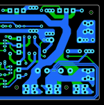
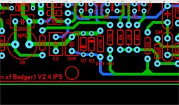
C114 should not go to speaker ground.
I drew the current loops again... It looks like 2.1.0 is actually the best again. This actually surprised me. And it looks like the ground traces should just go straight to the speaker ground as the excursion deep into the heart of the PSU loop is likely worse than the minor ground potential caused by the speaker current through the trace from G1 to the speaker terminal. It would be sufficient just to make this trace as fat as possible. I know this goes against my earlier advice... But these current loops are like some kind of chinese torture puzzle. I'm sure someone could turn this into a puzzle game people could play on their phones.
The lytic traces however should not be any wider than necessary, as current flows somewhere between the middle of the trace and the inner edge of the loop due to eddy currents. When you widen the traces you increase the loop area because the currents want to follow the middle of the trace to some extent.
Stuart, my condolences to your continued sanity. I don't know if you realized what you signed up for... But if it's any comfort this is exactly what I go through when I do this.
Attachments
Thanks for that Assessment KT. I believe that following your wonderful sketches that I could decrease the loop area even more in V2.3.0 It does however mean that the user would need to tap an extra hole or use the pcb stand off. To be honest there's a lot more difficult things to do when building an amplifier than tapping one M3 hole. They will need to do the VBE one anyway so what's the difference in tapping one more.C114 should not go to speaker ground.
I drew the current loops again... It looks like 2.1.0 is actually the best again. This actually surprised me. And it looks like the ground traces should just go straight to the speaker ground as the excursion deep into the heart of the PSU loop is likely worse than the minor ground potential caused by the speaker current through the trace from G1 to the speaker terminal. It would be sufficient just to make this trace as fat as possible. I know this goes against my earlier advice... But these current loops are like some kind of chinese torture puzzle. I'm sure someone could turn this into a puzzle game people could play on their phones.
The lytic traces however should not be any wider than necessary, as current flows somewhere between the middle of the trace and the inner edge of the loop due to eddy currents. When you widen the traces you increase the loop area because the currents want to follow the middle of the trace to some extent.
Stuart, my condolences to your continued sanity. I don't know if you realized what you signed up for... But if it's any comfort this is exactly what I go through when I do this.
It is not possible to connect C114 directly to PSU ground. So I'll leave it up to OS as to what version he wants to move forward with. Personally I will be building V2.3.X once I tweak it based on the updates done to V2.4
So I'll send you some of these boards too, as a token of my appreciation for your support during this project.
It does however appear that we are just about at RTM. Hooray.
I'll tweak V2.3.0 tonight to make the changes and reduce the loop area as far as I can.
Last edited:
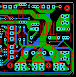
I would tweak V2.2.0 to reduce the loop area:
- move R126+L1 towards left as much as possible
- cancel TP3 (maybe find place later, above ouput zobel, closer to TP2)
- move the output terminal up, in line with R126+L1
- move SPK_GND up, as much as possible
- connect it to G1 with wire above C117
- connect GND Lift+G1 G2 wires to G1 with wire above C116, as close to the fedback wire as possible.
- C113 GND side can be connect to the speaker GND, as it is practicalli parallel with the load, so you can drive it on the right side of output terminal
I hope it is good idea. I'm not able to check it, as I use Eagle.
Sajti
C114 should not go to speaker ground.
I drew the current loops again... It looks like 2.1.0 is actually the best again. This actually surprised me. And it looks like the ground traces should just go straight to the speaker ground as the excursion deep into the heart of the PSU loop is likely worse than the minor ground potential caused by the speaker current through the trace from G1 to the speaker terminal. It would be sufficient just to make this trace as fat as possible. I know this goes against my earlier advice... But these current loops are like some kind of chinese torture puzzle. I'm sure someone could turn this into a puzzle game people could play on their phones.
The lytic traces however should not be any wider than necessary, as current flows somewhere between the middle of the trace and the inner edge of the loop due to eddy currents. When you widen the traces you increase the loop area because the currents want to follow the middle of the trace to some extent.
Stuart, my condolences to your continued sanity. I don't know if you realized what you signed up for... But if it's any comfort this is exactly what I go through when I do this.
Phone game , huh ?
I'm on it now ...
I'm already insane ... continued insanity is normal.
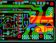
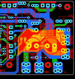
(below) is the grounding and a cleaned up power zone. The via's are the
true G1 now. The two grounds to "Canada" now go to speaker ground.
So , just move the NFB back above the coil and loop around the output pad ??
Yeah , Glift is also in error. Clift and Rlift must go to the long "canada"
trace. so do the 2 diodes (D1/2).
A 14 pin DIP also might be problematic for the IPS's , I'm looking into
the real creep requirements for each of my connections at the interface.
I even think JW's grouping of NFB/PD+/ND- is the way to go since .254
pitch is so common. I could even just group PD+/ND- together to keep
NFB and its return together. My goal is to get back to a 12 position unit.
OS
Attachments
KT , why not PSU ground as the take-off. Would it not be the most rock
solid ground on the the whole layout ?
OS
solid ground on the the whole layout ?
OS
Please explain to me what lytic traces are as I have no concept of what your talking about. Lol....
Returns to what?C115/117 returns.
Returns to G1 or returns PSU GND?
Thanks for that Assessment KT. I believe that following your wonderful sketches that I could decrease the loop area even more in V2.3.0 It does however mean that the user would need to tap an extra hole or use the pcb stand off. To be honest there's a lot more difficult things to do when building an amplifier than tapping one M3 hole. They will need to do the VBE one anyway so what's the difference in tapping one more.
The hole for the VBE transistor is part of the UMS so no drilling and tapping is required for it.
Returns to what?
Returns to G1 or returns PSU GND?
A picture is worth a thousand words.
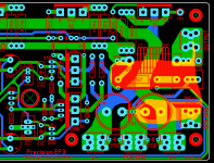
I think I've integrated KT's wonderful madness and will also integrate
JW's. 😀
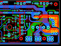
PS corrected below with -
-NFB through a VIA looping around L1/output.
-smaller C115/117 traces going to G1 via(s).
-G2 and Glift are drawn off the speaker ground return that also terminates
to the 6 vias.
-Zoble goes to vias.
-C114/116 go to PSU ground.
This seems to cover all that KT mentioned. (with extras).
The 6 vias should be 25A+ capacity.
OS
Attachments
Nice work OS.A picture is worth a thousand words.
I think I've integrated KT's wonderful madness and will also integrate
JW's. 😀
PS corrected below with -
-NFB through a VIA looping around L1/output.
-smaller C115/117 traces going to G1 via(s).
-G2 and Glift are drawn off the speaker ground return that also terminates
to the 6 vias.
-Zoble goes to vias.
-C114/116 go to PSU ground.
This seems to cover all that KT mentioned. (with extras).
The 6 vias should be 25A+ capacity.
OS
So by using the vias you can ensure that current and voltage is converging on G1.... love it!
Can you email me the file once your done and KT and JW's have verified what you have done so I can go over it again my end.
Last edited:
Shouldn't the ground trace from the Zobel be wider?
R113 could be moved down beside R110 to shorten up some power traces.
R113 could be moved down beside R110 to shorten up some power traces.
Yeah , JW. Did that. 1.5mm trace ... if the Zobel overloads that ... somethings
wrong.
All done.
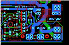
Glift was buggered.... 🙁 the 2 diodes , Clift and Rlift resistor must go
to the return trace direct. the other side of those 4 components is the
true lifted ground that C2/R2 and the rest of the LTP reference to.
(below 1 - fixed).
PD+/ND- are together 4V , no creep.
(below 2).
NC's between any HV are 2X .6mm creep for 1.2mm with NFB being the
worst case at 110VAC potential.
DIP was not centered , now it is a 12 position with row 2 @2.54mm from the edge. I have 3 IPS's done .... it must match.
OS
wrong.
All done.
Glift was buggered.... 🙁 the 2 diodes , Clift and Rlift resistor must go
to the return trace direct. the other side of those 4 components is the
true lifted ground that C2/R2 and the rest of the LTP reference to.
(below 1 - fixed).
PD+/ND- are together 4V , no creep.
(below 2).
NC's between any HV are 2X .6mm creep for 1.2mm with NFB being the
worst case at 110VAC potential.
DIP was not centered , now it is a 12 position with row 2 @2.54mm from the edge. I have 3 IPS's done .... it must match.
OS
Attachments
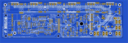
V2.42
wow , too many versions. 😛
Edit - Sip 1 header could of stayed 4 position. Emitters stay just .6V from output rail.
Unless something burns !! PS - 5 position is not stocked , unless you cut one.
OS
wow , too many versions. 😛
Edit - Sip 1 header could of stayed 4 position. Emitters stay just .6V from output rail.
Unless something burns !! PS - 5 position is not stocked , unless you cut one.
OS
Attachments
Last edited:
One quick thing, is the zobel capacitor rated for the max voltage swing at 100KHz? I fried some zobel capacitors. If you fry a zobel resistor and the capacitor is not rated for it, then you might replace the resistor without realizing the capacitor is also fried. Specifically it was a Kemet MMK capacitor I fried.
Last edited:
Yes , KT. The Zobel can be a very big HV unit.
I wanted to ask , I have the options of pulling G2/Glift (Canada traces)
from PS ground , speaker ground , or the G1 via's.
Are you sure speaker ground is best ?? The return of the speaker would be
in phase with output/ NFB at AF. Self hints at G1 for any aux. grounds. 😕
OS
I wanted to ask , I have the options of pulling G2/Glift (Canada traces)
from PS ground , speaker ground , or the G1 via's.
Are you sure speaker ground is best ?? The return of the speaker would be
in phase with output/ NFB at AF. Self hints at G1 for any aux. grounds. 😕
OS
- Home
- Amplifiers
- Solid State
- DIYA store "Wolverine" (Son of Badger) .... suggestions ??