I dont have 1.7mm holes. Here is an example of a 1.6mm hole.
Thats 2 five watts and a two watt in the same hole
Looks like the leads are 1mm.
Ahhh , worst case just use more solder for the bigger hole.
And , if you wanted to "piggyback" - lets say a 5pF lead cap on
R21 , it might fit.
Bigger hole is also more current passed through-hole D pie mm ...
1mm hole would be a 3.14mm trace. Wonder if the plated hole is 2oz. ?
OS
Does that mean diptrace is right ?
Those 2 big resistors (KOA and Vishay) are .8mm +/- .1mm. If those specs are right ... no issue w/ 1mm.
OS
.2mm clearance = .0078" in real measurements. That's way too tight. In machinist terms that's a slip fit for lubricated parts. Minimum clearance should be .015" for perfectly bent leads. Screw up the bend a couple times and get the leads distorted and it's a miserable go getting that to even fit. Go big!
For curiosity sake I've been flipping through a bunch of old files. Sizes were all over the place, but large. 1.7mm would be a the actual diameter of 16 gauge wire. On the Slewmaster 2 board the coil holes were 2mm. On the Slewmaster 2 the emitter resistors holes were 1.38mm. All the input boards I did use the Diptrace .500" LS 1/4W resistors. The inputs Jason did used 10.17mm LC 1/4W resistors with 1.02mm holes.
For some reason builders of the Honeybadger liked to go way oversize with the parts. 1/2W resistors and boutique input caps as big as your wrist. These are the builders who had the issue with parts fitting, not the ones using sensible parts. Best to plan for that.
For some reason builders of the Honeybadger liked to go way oversize with the parts. 1/2W resistors and boutique input caps as big as your wrist. These are the builders who had the issue with parts fitting, not the ones using sensible parts. Best to plan for that.
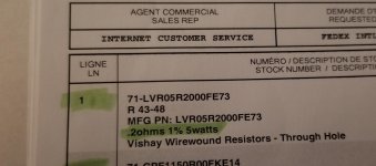
For my Badger, I used mostly KOA 1/4 or even 1/8 for some I believe. Unless other wise called for by OS. Everything fit really well. I remember having trouble with one part, I believe it the was dale vishay .22 5W resistors , and that was due to lack of stock in other resistors, but I can't recall for certain.
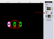
Wolverine bighole...
Does not look bad.
At actual size , it kind of looks right.
I'm thinking of hole -less SMD now.
OS
Does not look bad.
At actual size , it kind of looks right.
I'm thinking of hole -less SMD now.
OS
Attachments

Last edited:
Do you remember the part number for the Dale .22 resistors, or can you get a quick diameter measurement?
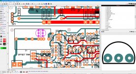
Good work Guys.
The board is ready coming together.
Can we please increase the size of the pads on the transistors.View attachment 941137
The board is ready coming together.
Can we please increase the size of the pads on the transistors.View attachment 941137
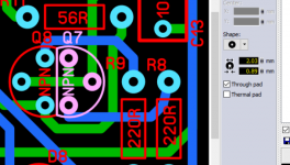
Can't we assume people will use formed leads. If not they can bend them. Formed leads obviously helps with creepage etc.There's not enough space between the leads for larger pads. I found one of my Kypton-ND layouts that I did in sprint. It used a different macro with 2.504 lead grid spacing.

I'm trying to figure out how to do that. I haven't used Sprint for years, I need to figure it out again.
If I recall correctly Phillips recommended going to the .100"/2.54 lead spacing years ago for the extra creepage distance.
Do you remember the part number for the Dale .22 resistors, or can you get a quick diameter measurement?
Part number attached. I don't have access to the amp to measure until tomorrow.
Attachments
Can't we assume people will use formed leads. If not they can bend them. Formed leads obviously helps with creepage etc.View attachment 941143
I think stuart is right it will help with the creepage also it would be better 2.54 mm formed leads are really easy to insert in a straight line what you guys think?
Attachments
Last edited:
I suck at Sprint! We'll have to see what the master says with the footprint change. It'll take some work. Straight line are easy to insert, but also easy to bend if bumped. I usually use that format myself though.
is not so difficult I spend I think like a few years learning 😛 by the way OS is doing the changes we are only here doing suggestions a bit, he is the driver of the project, in my opinion looks so good already 🙂
For Sprint, use Alt to select individual pads in a component and you can then change that without the whole object. I have developed models for splayed legs of TO92 devices. You just need to modify the border of the transistor outline if you decide to use thru-hole pads as thru-hole pads should not have silkscreen over them as per the DRM parameters.
That looks better OS,
This is my preferred macro for TO-92 with formed leads.
I have also attached all the other ones I have for future reference.
Just hold down Alt to select and edit individual components within a macro.
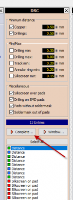
You may want to run a DRC check with these settings just to get an idea of close traces and if there is any silkscreen over pads etc.
It did find 13 entries.
Enjoy
This is my preferred macro for TO-92 with formed leads.
I have also attached all the other ones I have for future reference.
Just hold down Alt to select and edit individual components within a macro.
You may want to run a DRC check with these settings just to get an idea of close traces and if there is any silkscreen over pads etc.
It did find 13 entries.
Enjoy
Attachments


Last edited:
- Home
- Amplifiers
- Solid State
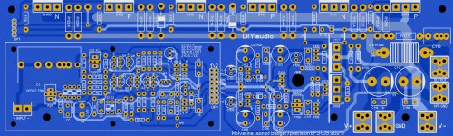
- DIYA store "Wolverine" (Son of Badger) .... suggestions ??