What about a helper transistors for the current mirror to help keep the balance of the currents closer and improve the transfer functio. It also causes the collectors of both IPS transistors to be at the same DC potential.


Last edited:
Final - all of it .... except for mistakes.
ALL the work. (below)
I appreciate the design suggestions , "diminishing returns" ....
This is why the project is open ended. With a 50 X 120mm addon board ,
design a 50 semi SMD - plug it in.
It was informative ....
- Really learned the Servo - got a better one.
- Added two pole compensation.
- Lifted ground , fat power terminals.
- MUCH better looking drafts !!
Any mistakes , please comment.
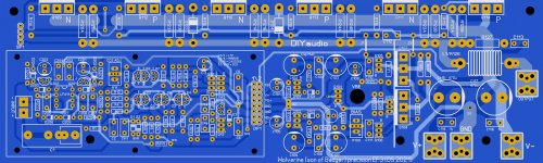
Below is LT/sprint + pix ..
I just did the servo section , still checking for errors.
OS
ALL the work. (below)
I appreciate the design suggestions , "diminishing returns" ....
This is why the project is open ended. With a 50 X 120mm addon board ,
design a 50 semi SMD - plug it in.
It was informative ....
- Really learned the Servo - got a better one.
- Added two pole compensation.
- Lifted ground , fat power terminals.
- MUCH better looking drafts !!
Any mistakes , please comment.
Below is LT/sprint + pix ..
I just did the servo section , still checking for errors.
OS
Attachments
Peter,
That's a beautiful pcb and really competent power amp.
I wouldn't change a thing!
Take a bow........
Hugh
That's a beautiful pcb and really competent power amp.
I wouldn't change a thing!
Take a bow........
Hugh
Hi OS,
After my discoveries with my test HB board.
Do you think output drive current from the VAS would be better if the emitter resistor R19 was around 10 ohms. I found this was the optimal value from my HB testing.
After my discoveries with my test HB board.
Do you think output drive current from the VAS would be better if the emitter resistor R19 was around 10 ohms. I found this was the optimal value from my HB testing.
Everybody wants everything !!
I do see Q10's collector not hooked to the rail. I suppose I must change
that.
10R for R19?? That would depend on the device , do we really need much
current ? This is not a EF2. Badger needs current , that EF2 can load mA's
from the VAS.
This EF3 loads at under 50uA /100Vp-p 2R. This why I see no change. VAS is unloaded and
pretty much isolated from any load.
Thank you , Hugh.
OS
Nice.... So now that the design is finished. Will you put a BOM together from digikey or mouser?
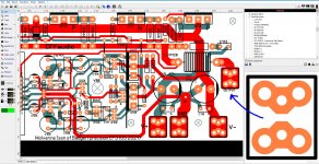
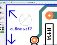
hi wow that look so good I'm gonna spend time looking at it OS also I like this idea of PCB that can use other IPS designs there with stand off nice, so I see 120 mm x 49.500 mm 🙂 ohhh terminal screw I see you 😛 also no outline yet still on revision?
edited: ohhh got it "I just did the servo section , still checking for errors. OS"
edited: ohhh got it "I just did the servo section , still checking for errors. OS"
Attachments
Last edited:
Some questions while everyone is here.
1. What type, voltage, pitch capacitor is ideal for the Zobel. Capacitor rated for AC or DC.
2. As for the 100nF decoupling capacitors, is it better to use X7R here or Wima film caps ?
Regards
1. What type, voltage, pitch capacitor is ideal for the Zobel. Capacitor rated for AC or DC.
2. As for the 100nF decoupling capacitors, is it better to use X7R here or Wima film caps ?
Regards

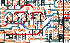
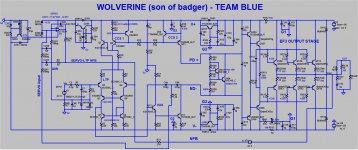
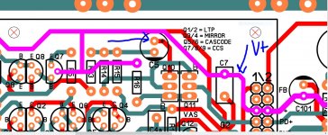
Nice work Juan, your sprint layout skills are awesome.OS I think I found a little text error Q3 and Q6 bases are connected when I was looking at the schematic I got lost 😛, I saw Q5 and Q6 face to face and I be like ? I be like hold on Q5 should be with Q4 right?
Can we increase some of the pad sizes?


that can be done sure the pads, I notice this too, is Q10 emitter suppose to go to V+ rail right? is not connected there? I see Q10 emitter to C5 and stop right there 🙁, C5 =10uF and C7=100nF ID updated 🙂, the pads size can be change later, lets help Ostripper find little bugs the best we can ST 🙂
Attachments
Last edited:
OS I think I found a little text error Q3 and Q6 bases are connected when I was looking at the schematic I got lost 😛, I saw Q5 and Q6 face to face and I be like ? I be like hold on Q5 should be with Q4 right?
Layout - Looks right to me.
Q5/3 are reversed on the schema. Thanks.
Should Go 1/5/3 on the input side , 2/6/4 on the NFB side.
R8 is Q4's Re , R7 is Q3's
Q5/6 bases are buffer divider R5/6.
Updated Schema below.
OS
Attachments
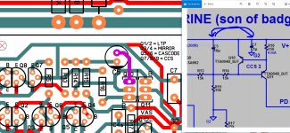
that can be done sure the pads, I notice this too, is Q10 emitter suppose to go to V+ rail right? is not connected there? I see Q10 emitter to C5 and stop right there 🙁, C5 =10uF and C7=100nF ID updated 🙂, the pads size can be change later, lets help Ostripper find little bugs the best we can ST 🙂
I got that one last night. Q10 C goes top foil to + of C3 then bottom side to rail.
Tiny 3mm trace was lost - oops.
Thanks.
OS
Why would you ask me this ??
450 uA per rail. They are not shunt regs. That is 25mW.
By that logic every KSA992 on the board would blow.
Cascode 992's use 92mW. 992 is rated 500mW.
Q8 = 3.2ma @ 58 Vce .... it runs cold at 185mW.
In the real world , I've built these regs- used with 45V rails..
1845/992's ran COLD !!
Previously used Zener shunts , those ran hot. Especially the resistor.
PS - You could even use TO-92's for the main ripple eaters. 2V drop/15mA - 30mW.
But I like overkill - TO126. Startup inrush might come closer to the 992's rating.
OS
Last edited:
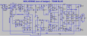
What about a helper transistors for the current mirror to help keep the balance of the currents closer and improve the transfer functio. It also causes the collectors of both IPS transistors to be at the same DC potential.View attachment 939118View attachment 939119
OS you don't like this suggestion?
Also I cannot tell what the lead pitch is for C113. Can you make it variable like R127, that it's connected to? My preference is to use a large plastic cap at the output in case of oscillation etc?
Thanks for another wonderful design.
I liked it a lot. But just make yer 50 X120 board.
The helper tightened up the mirror from mV to uV/uA-nA. But , not much
in the way of THD/offset inprovement.
You want a big Zoble , sure .... Ya think it might oscillate ??
OS
The helper tightened up the mirror from mV to uV/uA-nA. But , not much
in the way of THD/offset inprovement.
You want a big Zoble , sure .... Ya think it might oscillate ??
OS
- Home
- Amplifiers
- Solid State
- DIYA store "Wolverine" (Son of Badger) .... suggestions ??