ANOTHER LEVEL...
Let them make fun of my through -hole.
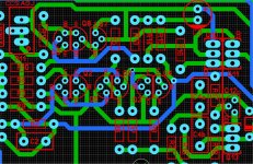
Another level of perfection , check out that IPS/VAS (below).
It will preserve 2ppm , I think ...
I port this to my hawksford VAS in the SMD greenamp.
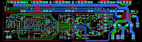
Layout style is not supported on autoroute. Autoroute
is 20 years in my brain. AI might get it someday , but not today.
OS
Let them make fun of my through -hole.
Another level of perfection , check out that IPS/VAS (below).
It will preserve 2ppm , I think ...
I port this to my hawksford VAS in the SMD greenamp.
Layout style is not supported on autoroute. Autoroute
is 20 years in my brain. AI might get it someday , but not today.
OS
Attachments
Wow , 1206 LED's are .11c each.
If you're looking for LED's look at Wurth Leds, they provide ltspice models for both their through-hole and smd leds.
Wurth SMD Leds - use 1206_150120GS75000 for smd green and 1206_150120RS75000 for red led. I used these in ltspice for smd spooky.
Wurth Through-Hole Leds
Wurth Through-Hole Leds Waterclear
Click on downloads in the table to find the ltspice models.
I am with Pete, Kicad is very good, but the learning curve is ultra steep and even the free program that it is, leaves a lot to be desired. Any suggestions on a good class/Youtube or such would be welcome.
Layout gets the job done now. And I will stick with it for now.
Layout gets the job done now. And I will stick with it for now.
Last edited:
This is the set of videos I have been watching to slowly learn Kicad:
KiCad 5 Tutorial - YouTube
These videos so far have been easy to follow, and cover Kicad 5 instead of older versions.
I remember trying Kicad 4 and giving up, Kicad 5 is a little easier to figure out.
KiCad 5 Tutorial - YouTube
These videos so far have been easy to follow, and cover Kicad 5 instead of older versions.
I remember trying Kicad 4 and giving up, Kicad 5 is a little easier to figure out.
C2 and R2 are connected to supply ground. The schematic is showing them connected to the ground lift resistor. Which one is correct?
Should the servo ground reference be connected to supply ground or the lifted input ground? If I recall correctly Thimios saw a substantial difference in distortion levels by connecting it to the lifted ground on Spooky.
Should the servo ground reference be connected to supply ground or the lifted input ground? If I recall correctly Thimios saw a substantial difference in distortion levels by connecting it to the lifted ground on Spooky.
On the top side of the servo, + & - inputs are connected together. I think it's supposed to be + & out but I can't make out the schematic properly.
C2 and R2 are connected to supply ground. The schematic is showing them connected to the ground lift resistor. Which one is correct?
Should the servo ground reference be connected to supply ground or the lifted input ground? If I recall correctly Thimios saw a substantial difference in distortion levels by connecting it to the lifted ground on Spooky.
Servo reference difference. This must be a real world phenomena.
Any suggestions ??
I have the options of either lifting the whole IPS or any of the 4 starred
ground references.
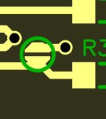
I did fix the Q6 and R3/4 (below).
Photo shot looks pretty - where do I buy one ??
I was also looking at the Board to board connectors on Mouser , Soooo
many choices.
OS
Attachments
On the top side of the servo, + & - inputs are connected together. I think it's supposed to be + & out but I can't make out the schematic properly.
Ohh .. that one hid from me , you are right.( - /out) shound be bridged. That
op-amp is just in a buffer/follower mode.
Other one is an active non-inverting LPF.
Thanks , JW.
PS - I'm making a book (PDF) , I will acknowledge your layout assistance.
OS
Last edited:
Hopefully Thimios can remember what he found for sure with the servo. It was a couple years ago, I may be remembering incorrectly. Your B side of the servo looks like it's still wrong.
I can order a small batch of boards and send some testers your way if you like. I get a frequent flier discount through PCBWay.
I can order a small batch of boards and send some testers your way if you like. I get a frequent flier discount through PCBWay.

.
Photo shot looks pretty - where do I buy one ??
I was also looking at the Board to board connectors on Mouser , Soooo
many choices.
OS
JLCPCB are "cheap" PCB manufactures.
Hopefully the connector that is chosen is not made from steel.
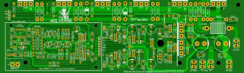
That's looking good! I see you added some screw holes for the input boards too.
It just dawned on me there's no way to run the input stage in isolation unless the output stage is left unpopulated.
It just dawned on me there's no way to run the input stage in isolation unless the output stage is left unpopulated.

That's looking good! I see you added some screw holes for the input boards too.
It just dawned on me there's no way to run the input stage in isolation unless the output stage is left unpopulated.
Sort of a half - solution to that .... G2 and NFB via's can be drilled to not allow
stray ground or NFB signals if using a separate input stage.
Input stage in isolation ??? I've done that powered right off the slewmaster.
- 2X 2.7K's between PD+/12V+ and ND-/12V-. Output stage is populated and
running a static 50ma bias - no input stage required.
Then , 2X 1K's in series across PD+/ND- (IPS) , run the centerpoint to NFB.
This won't work with any CFA's low Z. Works with all VFA's.
Jacks near the two LED's facilitate this (below).
PS - hopefully builders would make the onboard or 3'rd party choice right off the bat.
I might clone the onboard IPS to a 50mm X 100mm PCB , just for that purpose.
I won't force anybody into the modular way.
OS
Attachments
Last edited:
Please ignore if this isn't helpful or has already been considered...
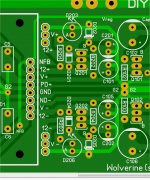
But would there be any negative effect if the 8 solder pads for the daughter boards pin connector (coming from the IPS) were doubled up/ done in two rows? This would offer the ability to jumper for on board use, or solder a connector for daughter cards, ignoring the second row.
But would there be any negative effect if the 8 solder pads for the daughter boards pin connector (coming from the IPS) were doubled up/ done in two rows? This would offer the ability to jumper for on board use, or solder a connector for daughter cards, ignoring the second row.
Ahhh , not helpful ??
That is brilliant !!!!! 🙂🙂🙂
I was just looking at dual SIP molex connectors.
Did not really make that connection (pun intended).
I could put a male dual row onboard. they would either jumper the dual
row for onboard with a bridged female or just engage the OPS facing row
to go outboard (single row female).
PS - there is nothing really tall in the IPS section (8mm C3 ??)
Canadians "think outside the box"
OS
I prefer to put the female connector on the board with the power supply. It's a little safer that way, no exposed high voltage pins. The two row jumper would work though.
Another option is a small solder blob jumper to activate/ deactivate a trace. I use them for address selection for I2C devices, but they work well for disconnecting supply regulators. ect in big SMT boards.
Another option is a small solder blob jumper to activate/ deactivate a trace. I use them for address selection for I2C devices, but they work well for disconnecting supply regulators. ect in big SMT boards.
Attachments
- Home
- Amplifiers
- Solid State
- DIYA store "Wolverine" (Son of Badger) .... suggestions ??