Hi Greg,
.36V across 100R is high. That is .36V/100R= .0036A. The TDA1541A current offset should be .002A.
I don't know whether the high voltage damaged it. I don't have any experience with that. Did you test the chip in a working dac prior to installing it in the D3 board? Do you have another TDA chip to test the D3?
Years ago when I first started building my own dac, I purchased a couple of cheap TDA1541 (non-A) chips for testing purposes so that I did not have to test using my more expensive chip.
Ben
Yeah, I had to learn the hard way. I just ordered another S1 and I will be using my R1 until this design is known to be good!
I think a build manual would have been really helpful.
Cheers,
Greg
Greg,
That's good news and unfortunately bad news.
On the other hand, the dac still sounds good with a lesser chip.
Ben
That's good news and unfortunately bad news.
On the other hand, the dac still sounds good with a lesser chip.
Ben
Ben,
Well, at this point I have one channel that is good (left) and still cannot get the offset out of the right (60mv). However, the bigger problem is that I cannot get any audio out of the one good channel. I've got the board set for I2S, bypassing the Simultaneous board, and going directly from my Singxer USB -> I2S board.
I use a Linux OS (Euphony Symphony -> Roon), and the USB converter board shouldn't need any drivers. The board gets properly identified and shows that it is "playing." But, I get nothing.
I can understand that the board would not do I2S in Simultaneous, but should it not work in straight I2S mode???
Again, here is my board:
Singxer C-1 XMOS Digital Interface XU208 U8 Upgraded Femtosecond TCXO Audio | eBay
Stumped and confused 😕
Cheers,
Greg
Hi Greg,
You had previously checked the output bias circuitry and it was working correctly. As for your R1 chip, you said that it was measuring 0.2V across the IV resistor when R32 and R33 were removed. Did you get 0.2V at both channels? I'm just wondering why one channel does not zero.
As for I2S input, did you solder J1 for input selection on the back of the board, with no solder on J2 or J3?
If J1 is selected, the next thing to check is to see if the I2S signals are getting to the chip. The U.FL are small and too much solder can short them at the pads. Check each with your ohmmeter to make sure that the centre pin is not shorted to ground. Also check that the soldering of all of the resistors and diodes near pins 1 to 4 (data input pins) are OK.
You might be able to check for AC voltage (mV) at pins 1, 2, and 3 of the TDA socket with the TDA removed. I am not sure how reliable that is though. I have an oscilloscope and I know that using it to check for digital signals does work.
Ben
Ben,
Yes, I have done everything, j2 and J3 are open, J1 is closed.
I will check with a an ohmmeter the U.FLs and pins 1,2, 3.
Thank you,
Greg
Yes, I have done everything, j2 and J3 are open, J1 is closed.
I will check with a an ohmmeter the U.FLs and pins 1,2, 3.
Thank you,
Greg
Ben,
I just found that the LE anode is grounded. That was the very first U.FL that I soldered, so, looks like I bridged the pads underneath!.
Also, I measured ~430 ohms between BCK anode and ground. Shouldn't this 470?
Data Left / Data and Data Right are open. Shouldn't they all be ~R470 to ground, based on the schematic?
At least I found some glaring problems...
Cheers,
Greg
Hi Greg,
At BCK there are other components that are connected that would affect the resistance, so I would not worry about it for now.
If DL and DR are completely open, it could be bad solder joints. It is best if you reflow the joints with a soldering iron. I had to do that with my board as I had one or two joints that were not good. Again, there are multiple components so working out the resistance is not so simple. The aim is to get to a point where you can measure some resistance, not infinite resistance or short.
WS1 has diodes so use the diode test on your multimeter to test for continuity and good solder joints.
Once you think all joints test good, you can try powering it up again.
Ben
Ben / Ryan,
Could you please measure LE on the D3 anode to ground and tell me what you get? I'm getting some 19mOhm. Maybe D1 is causing it to measure that high?
Testing WS1 with diode check yields .000v. Good.
Still no sound. I don't have a scope to see if data is getting to the chip.
Cheers,
Greg
Could you please measure LE on the D3 anode to ground and tell me what you get? I'm getting some 19mOhm. Maybe D1 is causing it to measure that high?
Testing WS1 with diode check yields .000v. Good.
Still no sound. I don't have a scope to see if data is getting to the chip.
Cheers,
Greg
Hi Greg,
At WS1, with diode check (TDA installed), positive probe at TDA pin 1, negative probe at other end of diode D1, V=0.59V, R=1.62Mohm, reverse probes V=0. What do you measure with positive probe at chip end of D1?
I was not able to access the underside of my board to measure D3. With TDA installed, with negative probe at TDA pin 1 and positive probe at Gnd (D2, D4, D3 in series), 1.2kohm, 1.015V. With positive probe at pin 1 and negative probe at Gnd, 1.2kohm, 1.27V.
Ben
Greg,
If you post detailed pictures of both sides of the D3 board, perhaps Ryan might see something.
Ben
If you post detailed pictures of both sides of the D3 board, perhaps Ryan might see something.
Ben
Early stages
Wife has gone away for work therefore ... the dining table is mine for the whole week!! should be well towards being finished by then.
So far in donor Onkyo chassis (be long term home but maybe not forever as I have other ideas)
Sjostrom SSR03 At 30v to power B1 output
3 x 5v Reflecktor-D = 2 for Receiver, 1 for I2S to Simultaneous
1 x 8v for the D3 board
I plan to fit D3, I2S and receiver vertically on back panel
Attachments
1 x 8v for the D3 board
Ok just had another look because I have D2 and D3 and now remember that D3 needs 5v not the 8v from D2
And D3 board is bigger than D2 so it is not going to fit as planned - back to the drawing board
Happy with my days work.
All the drilling etc complete.
I had some ridiculously oversize output caps on the D1 and so this was giving me grief trying to fit everything in - so I swapped them out for some smaller ones which gained me more real estate
Wire up my psu and regulators tomorrow. I’ve tested them all separately already so hopefully there will be no problems. Only the D1 is completely untested.
Attachments
Hi Greg,
At WS1, with diode check (TDA installed), positive probe at TDA pin 1, negative probe at other end of diode D1, V=0.59V, R=1.62Mohm, reverse probes V=0. What do you measure with positive probe at chip end of D1?
I was not able to access the underside of my board to measure D3. With TDA installed, with negative probe at TDA pin 1 and positive probe at Gnd (D2, D4, D3 in series), 1.2kohm, 1.015V. With positive probe at pin 1 and negative probe at Gnd, 1.2kohm, 1.27V.
Ben
Ben,
This is very helpful. When I get home on Wednesday I’ll check again, but I think D1 might be reversed.
I did have WS1 shorted, fixed, but I really need to replace a couple of the U.FL.s
I will post detailed pics as well.
Thank you for all the help!
Ryan,
How is your D3 board stock at this time?
Cheers,
Greg
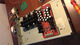
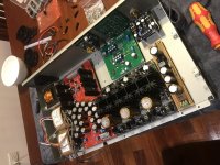
This obviously is not the pictures you need, but this is my build.....

My phone inserts all of inverted...sorry. That's the the way I like to fly, though.
I will get the D3 working, I will not fail!!
My phone inserts all of inverted...sorry. That's the the way I like to fly, though.
I will get the D3 working, I will not fail!!
Last edited:
Sthcoaster... looks great!
Greg... looks like you are on the right path. Basically, if you have +5,-5.-15v at the 1541a, AND a proper digital signal, the 1541a will make music. (if it sounds bad then problem is with caps or DEM). So if you are missing music it is the signal that is the problem. Trace back to the source and you will succeed. Best luck.
Greg... looks like you are on the right path. Basically, if you have +5,-5.-15v at the 1541a, AND a proper digital signal, the 1541a will make music. (if it sounds bad then problem is with caps or DEM). So if you are missing music it is the signal that is the problem. Trace back to the source and you will succeed. Best luck.
Sthcoaster... looks great!
Greg... looks like you are on the right path. Basically, if you have +5,-5.-15v at the 1541a, AND a proper digital signal, the 1541a will make music. (if it sounds bad then problem is with caps or DEM). So if you are missing music it is the signal that is the problem. Trace back to the source and you will succeed. Best luck.
Thanks for the encouragement. I’ve pretty much made all the mistakes
 So, I will be putting a guide together to help prevent others from making all my mistakes!
 Yes, I will get there. I just ordered fresh PCB, I may start over. I think I’ve got a reversed diode on WS1.
Cheers,
Greg
Hi everyone,
Thank you for all the help! I got home today and my cheap Digital Coax to I2S converter came. So I hooked it up and checked all supply voltages which have always been spot on and everything looked good.
I had no connections for signal input or output. This was the key for me! Everything connected and it works perfectly!!!!!!
AOL & AOR are zeroed with equal positive and minus variation across the 0V point.
Sound is very nice!
Thank you again,
Mark K.
Hi everyone,
Thank you for all the help! I got home today and my cheap Digital Coax to I2S converter came. So I hooked it up and checked all supply voltages which have always been spot on and everything looked good.
I had no connections for signal input or output. This was the key for me! Everything connected and it works perfectly!!!!!!
AOL & AOR are zeroed with equal positive and minus variation across the 0V point.
Sound is very nice!
Thank you again,
Mark K.
Good job!
Thanks Greg. I'm eagerly waiting for your posting the same conclusion, it does sound very nice and well worth it.
The Simultaneous board is also now in place and works very well too!
Mark K.
The Simultaneous board is also now in place and works very well too!
Mark K.
- Home
- Group Buys
- DIY TDA1541A PCB "D3"