DIY SCPI programmable dual channel bench PSU 0-50V/3A
List of important changes
Update 2015-02-14: New power pre-regulator schematic is posted here.
Update 2015-02-26: Corrected bias power supply schematic (Sheet 1) and simplified post regulator schematic (without TLC555/relay based bias control) is posted here.
Update 2015-03-21: Spice models added for redesigned power post-regulator.
Update 2015-04-06: Modified post-regulator Spice model with new OE circuit is added.
Update 2015-04-08: New schematics for pre-regulator and post-regulator and new PCBs are presented here.
Update 2015-05-15: Mosfet pre-regulator board is assembled and tested.
Update 2015-06-20: Eagle files, BOM and Gerbers for Pre-regulator PCB r2B5 (06/2015).
Update 2015-07-29: New PCB for front panel designed as Arduino shield for Mega2560 or Due boards is introduced. An 3.2" color TFT touch-screen display replaces monochrome 128x64 LCD. This PCB makes obsolete previous MCU board, 4x4 keypad and BP PCB.
Update 2015-07-30: New AUX power supply with soft-start/stand-by is added that make previous one obsolete.
Update 2015-10-03: SMD version of Mosfet pre-regulator board and post-regulator are assembled and tested.
Update 2015-10-21: Eagle files, BOM and Gerbers for the Arduino Shield latest revision
Update 2015-11-01: A new thread about software support for this power supply is opened here.
Update 2015-11-10: A repository for hosting hardware design files and source code is created and now available on https://github.com/eez-open
Redesigned PSU with smaller enclosure and SMPS pre-regulator
Update 2016-03-04: New power board (pre- and post-regulator merged into one)
Update 2016-03-05: AUX PS with fan controller, Ethernet and USB connection
Update 2016-03-05: Arduino shield with W5500 Ethernet controller
Update 2016-06-17: Redesigned set of PCBs for lower profile enclosure and hybrid power modules is available on the GitHub. This revision will be used for planned group buy.
Update 2016-10-06: Firmware M2 is released.
Update 2016-12-29: Firmware M3 is released.
Update 2017-02-23: EEZ H24005 became a fully funded campaign on the CrowdSupply.
__________________________________________________
Introduction
I’d like to present what I did until now trying to make a bench power supply that should have a solid “analog” core that can be enhanced by adding MCU for on-site or remote programming, monitoring and data logging. My understanding of analog circuits are basic and I tried to compile many ideas found on various places. Initial document was Agilent E3634A Service guide (Part No. E2634-90010, April 2000) and presentations found on i.e. Gerry’s and Ian’s blogs.
Presented work is still not backed by any simulation (I still wonder which one to choose, it that LTspice or something else, your recommendations are welcome). I can imagine that such simulation could save considerable amount of time and material.
There is many DIY power supply projects available (as cheap yet solid enough PSU that comes from various manufacturers) but I decide to try to make one by myself to learn a little about various circuits and parts that are now available on the market. The result of such quest is that I include many components that goes far beyond 2N3055 or LM317 based solutions but since we are in 21 century and logistics is amazing and since my budget is not so tight I think that I should proceed in that way. As a “reality check” to not end up with some really “esoteric” parts all what was selected has to be available through at least one of two European supplier (see below).
It’s also interesting that in DIY projects Vout of 30V is as some kind of magic threshold which is not cross over very often. Maybe it’s just a practical reason for that since most of today equipment do not need anything beyond 24V?
Situation with ideas about digital part and programming is better and many parts that is added on MCU board was inspired by my own view what kind of functionality programmable bench power supply should have. But this is a next step. The first one is to create solid core that can survive various testing torture and do not call into question safety/integrity of the various loads/equipment that could be connected somewhere in the future.
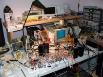
I spent many hours “breadboarding” and end up with complete mess (see picture of my desktop). Thanks to that many components was burned when I touch wrong wire or components or apply wrong voltage 🙁 So, it’s high time to put what is done on PCB. PCBs (see below) will be successors of the first batch where I mainly tested SMPS functionality that was previously unknown to me. On the beginning I tried to test LM5005 for bias, LM5118 for pre-regulator and LM5119 for both functionality since it is dual channel. Unfortunately I never succeed to do any testing with the latest for the simple reason that soldering QFN without reflow oven which I still don’t have became mission impossible despite some encouraging videos such as this one. Maybe the reason for my failure is not using of a solder paste but even if I succeed I start to wonder what kind of nightmare that may be for the other people who eventually decide to follow this project. Fortunately soldering (with the right soldering tip) of even tiniest SMD ICs (such as 5-pin SOT-23) become surprisingly simple.
In this first post I’d like to present some basic facts about projects such as goals, features, schematic and PCBs that I’m going to order soon. I hope that will generate discussion that will further improve this project even if that not necessary simplify something that one can already found too complex 🙂 Maybe we even ends up in not so distant future with group buy, who knows. Here we go:
Project goals list
PCB list
Modules feature list
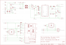
Power board
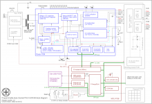
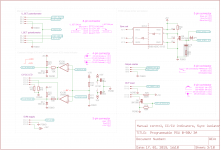
Schematic on Sheets 1/10 to 4/10
Most parts are tested. That also include basic ADC/DAC functionality (set Vout and Iout using DAC and measuring Vout/Iout using ADC). Require additional testing for pre-regulator tracker when pre-regulator enter buck-boost mode (Vin ≤ Vout). Currently design include a silly way of achieving power up and power down without overshooting regardless of the fact that load is connected or not. That is mainly because a bias supply with separate transformer (LM317/7805/LM339L) is used when experimenting and power-up sequencing is not correct (correct biasing comes too late despite of fact that pre-regulator has huge soft start of ~40ms).
During testing a LM5118 based pre-regulator was on the first PCB version. Power inductor in buck-boost can be under real stress and some of them (Bourns PM2110-820-K-RC1240) can reach, I believe due to the saturation (tested with Vin=40VAC and Vout=50V/3A), a temperature of 90oC or even more! The most flexible solution is playing with own inductor winded on the ETD ferrite core.
Low noise LDO (LT3030, TPS7A3001) in combination with SMPS pre-regulator (LM5574) was tested on breadboard only. That was pretty challenging and real performance (ripple rejection) was not possible to test.
For load/stability testing the following parts are used: 2 x 8R2/100W, 2 x 33/25W power resistors and 4 x 12V/35W halogen lamps. Tested with full 150W and beyond that (approx. 200W). Testing of two channels will be started when PCB arrived (then will be possible to test SMPS frequency sync and serial and parallel connection). I’d like to extend stability testing using 100R/25W resistor and DC motor (~100W).
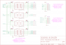
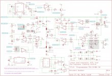
MCU board
Schematic on Sheets 5/10 to 7/10
Current status:
Not tested, require PCB
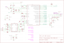
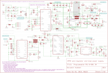
Aux power (+5V) and AC input protection
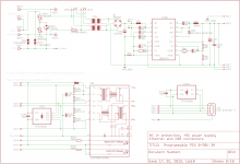
Schematic on the Sheet 8/10
Not tested, require PCB
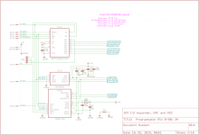
Binding posts
Schematic on the Sheet 9/10
Serial or parallel wiring of two Power boards without additional external cables using power relays
Sense to Output wiring without additional external cables using small signal relays
LED indication for mode of operation (serial/parallel) and Sense connection
MCU board is required for programming
LED and relay driver through 16-channel driver TI (TLC5925)
On-board protection against wrong programming to avoid simultaneous activation of serial and parallel relays (if serial mode is active parallel is automatically disabled)
DC outputs are guarded with combination of SAR, MOV and TVS
Current status:
Proof of concept tested (i.e. SPI communication with TLC5925 and serial/parallel relay control), more testing when MCU board become functional and two Power boards are assembled
4 x 4 Keypad
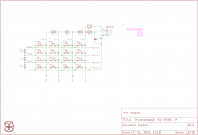
Schematic on the Sheet 10/10
Proof of concept tested, more testing when MCU board become functional
Ethernet + USB sockets board
Schematic on the Sheet 8/10
Not tested, require PCB
List of important changes
Update 2015-02-14: New power pre-regulator schematic is posted here.
Update 2015-02-26: Corrected bias power supply schematic (Sheet 1) and simplified post regulator schematic (without TLC555/relay based bias control) is posted here.
Update 2015-03-21: Spice models added for redesigned power post-regulator.
Update 2015-04-06: Modified post-regulator Spice model with new OE circuit is added.
Update 2015-04-08: New schematics for pre-regulator and post-regulator and new PCBs are presented here.
Update 2015-05-15: Mosfet pre-regulator board is assembled and tested.
Update 2015-06-20: Eagle files, BOM and Gerbers for Pre-regulator PCB r2B5 (06/2015).
Update 2015-07-29: New PCB for front panel designed as Arduino shield for Mega2560 or Due boards is introduced. An 3.2" color TFT touch-screen display replaces monochrome 128x64 LCD. This PCB makes obsolete previous MCU board, 4x4 keypad and BP PCB.
Update 2015-07-30: New AUX power supply with soft-start/stand-by is added that make previous one obsolete.
Update 2015-10-03: SMD version of Mosfet pre-regulator board and post-regulator are assembled and tested.
Update 2015-10-21: Eagle files, BOM and Gerbers for the Arduino Shield latest revision
Update 2015-11-01: A new thread about software support for this power supply is opened here.
Update 2015-11-10: A repository for hosting hardware design files and source code is created and now available on https://github.com/eez-open
Redesigned PSU with smaller enclosure and SMPS pre-regulator
Update 2016-03-04: New power board (pre- and post-regulator merged into one)
Update 2016-03-05: AUX PS with fan controller, Ethernet and USB connection
Update 2016-03-05: Arduino shield with W5500 Ethernet controller
Update 2016-06-17: Redesigned set of PCBs for lower profile enclosure and hybrid power modules is available on the GitHub. This revision will be used for planned group buy.
Update 2016-10-06: Firmware M2 is released.
Update 2016-12-29: Firmware M3 is released.
Update 2017-02-23: EEZ H24005 became a fully funded campaign on the CrowdSupply.
__________________________________________________
Introduction
I’d like to present what I did until now trying to make a bench power supply that should have a solid “analog” core that can be enhanced by adding MCU for on-site or remote programming, monitoring and data logging. My understanding of analog circuits are basic and I tried to compile many ideas found on various places. Initial document was Agilent E3634A Service guide (Part No. E2634-90010, April 2000) and presentations found on i.e. Gerry’s and Ian’s blogs.
Presented work is still not backed by any simulation (I still wonder which one to choose, it that LTspice or something else, your recommendations are welcome). I can imagine that such simulation could save considerable amount of time and material.
There is many DIY power supply projects available (as cheap yet solid enough PSU that comes from various manufacturers) but I decide to try to make one by myself to learn a little about various circuits and parts that are now available on the market. The result of such quest is that I include many components that goes far beyond 2N3055 or LM317 based solutions but since we are in 21 century and logistics is amazing and since my budget is not so tight I think that I should proceed in that way. As a “reality check” to not end up with some really “esoteric” parts all what was selected has to be available through at least one of two European supplier (see below).
It’s also interesting that in DIY projects Vout of 30V is as some kind of magic threshold which is not cross over very often. Maybe it’s just a practical reason for that since most of today equipment do not need anything beyond 24V?
Situation with ideas about digital part and programming is better and many parts that is added on MCU board was inspired by my own view what kind of functionality programmable bench power supply should have. But this is a next step. The first one is to create solid core that can survive various testing torture and do not call into question safety/integrity of the various loads/equipment that could be connected somewhere in the future.
I spent many hours “breadboarding” and end up with complete mess (see picture of my desktop). Thanks to that many components was burned when I touch wrong wire or components or apply wrong voltage 🙁 So, it’s high time to put what is done on PCB. PCBs (see below) will be successors of the first batch where I mainly tested SMPS functionality that was previously unknown to me. On the beginning I tried to test LM5005 for bias, LM5118 for pre-regulator and LM5119 for both functionality since it is dual channel. Unfortunately I never succeed to do any testing with the latest for the simple reason that soldering QFN without reflow oven which I still don’t have became mission impossible despite some encouraging videos such as this one. Maybe the reason for my failure is not using of a solder paste but even if I succeed I start to wonder what kind of nightmare that may be for the other people who eventually decide to follow this project. Fortunately soldering (with the right soldering tip) of even tiniest SMD ICs (such as 5-pin SOT-23) become surprisingly simple.
In this first post I’d like to present some basic facts about projects such as goals, features, schematic and PCBs that I’m going to order soon. I hope that will generate discussion that will further improve this project even if that not necessary simplify something that one can already found too complex 🙂 Maybe we even ends up in not so distant future with group buy, who knows. Here we go:
Project goals list
- “DIY friendly” – use THT components as much as possible, sockets for some ICs for experimenting with various solutions. Combine pinouts on PCBs of some components to host both SMD and THT variants, use jumpers and test points for simplified measurements
- Dual or single channel version
- Regulated voltage (CV) 0-50V, resolution 10mV
- Regulated current (CC) 0-3A, resolution 10mA
- SMPS buck-boost pre-regulator with output tracking control for lower power dissipation
- N-ch MOSFET based post-regulator
- Flexible main transformer output voltage rate (from 36-48VAC) using buck-boost mode of operation (output power when Vout > Vin limited mainly by allowable power inductor current)
- Main power inductor could be from various brands or custom made
- Over-current protection (OCP) for short circuit condition
- Easily modified for other ranges i. e. 0-30V or 0-5A
- Basic functionality has to be achieved with manual control without MCU board (set voltage and current, CC/CV indication, output enable, OCP reset)
- AC input protection (SAR, MOV, TVS)
- DC output protection (SAR, MOV, TVS)
- Simple serial (0-100V/3A) or parallel (0-50V/6A) connection of two power modules with tracking and LED indication (MCU controlled)
- Simple connection of Sense+/- outputs with LED indication
- Modular design that modules can be used in other projects
- Completely isolated MCU board signaling from analog section (Main power board) and PC
- SPI communication
- USB interface with ESD protection
- Ethernet interface with ESD protection
- Programming by Arduino sketches
- PC console for settings and monitoring
- Not using fan or other source of audible noise
- ADC and DAC resolution of min. 14 bits
- No power up or power down overshoot on the output (with or without load)
- Generate bias supply from main transformer (no aux transformer required)
- Single LCD 128x64 dot matrix for displaying all information for both channels
- 4 x 4 keypad + rotary encoder when controlled by MCU
- All components have to be available on Farnell element14 UK and/or (Transfer Multisort Elektronik (TMU.eu)). Presumably all selected components could be also found on Digikey and Mouser.
- Fit into metal case such as Modushop.biz (Hi-fi 2000) Economica EP1152820 L 280 x P 200 or Economica EP1153220 L 320 x P 200). Another possible source is Schaeffer (offer customized front panels and Alu cases).
PCB list
- Power board 0-50V/3A (two is required for dual channel version) – one PCB is mandatory for basic operation
- MCU board (piggyback on LCD) – offer MCU controlled mode of operation and PC connectivity
- Aux power (+5V) and AC input protection – supply for all MCU related PCBs
- Binding posts with connection LED indicators and DC output protection – optional, require MCU board
- 4 x 4 Keypad – mandatory for MCU mode of operation
- Ethernet + USB sockets board with protection – optional (can be replaced with some panel mounted sockets)
Modules feature list
Power board
Schematic on Sheets 1/10 to 4/10
- High voltage TI LM5118) buck-boost pre-regulator
- Support for the following power inductors: Vishay IHTH1125 series (THT), Bourns PM2120 series (SMD), Bourns 2300 series (THT), Murata 1400 series (THT), WE-HCI Flat Wire High Current Inductor (SMD) and vertical ETD 29/16/10 ferrite core (i.e. Epcos) for custom made inductor (use i.e. ExcellentIT inductor calculator, Inductor5200.exe)
- High voltage TI LM5574) bias SMPS and low noise positive LDO LTC (LT3030) for generating +15V and +5V and low noise negative LDO TI (TPS7A3001) for generating -15V (Ripple rejection should be around 50dB for selected SMPS working frequency of ~215 KHz!).
- TO220/FP power N-ch MOSFET and diode for SMPS for simple mounting on shared external heatsink
- Op amp based CC and CV control loops (TL074 is default, can be tested with other quad op-amp in DIP14 package)
- LTC6102) Precision Zero Drift Current Sense Amplifier
- Op amp based tracking control (inspired by the following design: Simple switchers make simple pre-regulators)
- DAC, 2-channel, 16-bits (TI DAC8552) provide U_SET and I_SET values simultaneously
- ADC, 4-channel, multiplexed, 15-bits (TI ADS1120). Two channels are used for measuring U_OUT and I_OUT another two are connected to U_SET and I_SET that comes from DAC and what can be used for some sort of auto-calibration.
- Precision +2.5V voltage reference with REF01 industry standard DIP8 socket for LTC LT1019-2.5) (comes with SMD adapters for LTC LT1790-2.5 or LT6654-2.5, TI REF5025 and TI LM4132)
- SMPS controllers frequency synchronization with isolation (Silabs Si8610) between Power boards and Aux power board for lowering EMI
- Test points for accurate measuring of input and output voltage and pre-regulator control loop and post-regulator CV control loop as suggested in TI snva364a
- Connector for U_SET and I_SET potentiometers (i.e. 50K multiturn) are provided in the fashion that manual or MCU control cannot be done simultaneously
- Connectors for OUT_ENABLE and OC_RESET switches
- Connector for OC LED
- Connector for CC and CV LED
- Connector for digital panel meter (eBay grade or perhaps from here) bias and U_OUT for manual operation (when MCU is not used)
- Buzzer for audible notifications and warnings
- SPI I/O expander (Microchip MCP23S08) is used for minimize required number of I/O lines (which has to be isolated!) between Power board and MCU board. Currently 7 out of 8 lines are occupied for CV mode (input), CC mode (input), OC reset (I/O), Power good (I/O), Pre-regulator enable (I/O), ADC DRDY (input) and OCP_ACTIVE (input).
Most parts are tested. That also include basic ADC/DAC functionality (set Vout and Iout using DAC and measuring Vout/Iout using ADC). Require additional testing for pre-regulator tracker when pre-regulator enter buck-boost mode (Vin ≤ Vout). Currently design include a silly way of achieving power up and power down without overshooting regardless of the fact that load is connected or not. That is mainly because a bias supply with separate transformer (LM317/7805/LM339L) is used when experimenting and power-up sequencing is not correct (correct biasing comes too late despite of fact that pre-regulator has huge soft start of ~40ms).
During testing a LM5118 based pre-regulator was on the first PCB version. Power inductor in buck-boost can be under real stress and some of them (Bourns PM2110-820-K-RC1240) can reach, I believe due to the saturation (tested with Vin=40VAC and Vout=50V/3A), a temperature of 90oC or even more! The most flexible solution is playing with own inductor winded on the ETD ferrite core.
Low noise LDO (LT3030, TPS7A3001) in combination with SMPS pre-regulator (LM5574) was tested on breadboard only. That was pretty challenging and real performance (ripple rejection) was not possible to test.
For load/stability testing the following parts are used: 2 x 8R2/100W, 2 x 33/25W power resistors and 4 x 12V/35W halogen lamps. Tested with full 150W and beyond that (approx. 200W). Testing of two channels will be started when PCB arrived (then will be possible to test SMPS frequency sync and serial and parallel connection). I’d like to extend stability testing using 100R/25W resistor and DC motor (~100W).
MCU board
Schematic on Sheets 5/10 to 7/10
- Atmel Atmega32u4 MCU
- EEPROM (up to 1Mb/128Kb x 8) for storing additional programming parameters and measurement data
- On-board RTC (NXP PCA 21125, http://www.nxp.com/documents/data_sheet/PCA21125.pdf) + 1F supercap (horiz. or vert. mounting) as backup power supply
- 2 x SPI communication ports (for two power modules) fully isolated using Silabs Si86xx (https://www.silabs.com/products/power/isolators/Pages/Si86xx-Digital-Isolators.aspx) high speed digital isolators. Communication ports follows10-pin ICSP port pinout (https://en.wikipedia.org/wiki/In-circuit_serial_programming)
- 1 x non-isolated SPI communication port (5V logic) for controlling Binding posts PCB
- 1 x non-isolated SPI communication port (3.3V logic) for external SDcard
- Support for Vishay LCD-128H064A (5V, controller Samsung KS 0107/KS 0108) and DOGL128 (3.3V, controller ST 7565R) 128x64 dot matrix display (works with only one at the time!). Both displays are supported in (U8glib)
- On-board Ethernet Microchip (ENC28J60). It’s possible to use its clock for driving MCU (f / 2) to avoid using two xtals (16MHz for MCU and 25MHz for Ethernet).
- On-board USB isolator (Analog ADUM3160)
- Support for two NTC for temperature measurement or one rotary encoder (currently same MCU pins are used)
Current status:
Not tested, require PCB
Aux power (+5V) and AC input protection
Schematic on the Sheet 8/10
- Provide power for the MCU and the Binding posts PCBs. Use the same SMPS controller (TI LM5574) as for bias power supply on the Power board. Can be in sync with other SMPS controllers on Power boards.
- Use PCB mounted transformer (9-15VAC). If two primary version is used, there is on board soldering spots for setting 115 or 230VAC. Another possibility is to make an auxiliary winding on main toroidal transformer by simply adding few turns over existing windings.
- AC input is guarded with combination of SAR, MOV and TVS
Not tested, require PCB
Binding posts
Schematic on the Sheet 9/10
Serial or parallel wiring of two Power boards without additional external cables using power relays
Sense to Output wiring without additional external cables using small signal relays
LED indication for mode of operation (serial/parallel) and Sense connection
MCU board is required for programming
LED and relay driver through 16-channel driver TI (TLC5925)
On-board protection against wrong programming to avoid simultaneous activation of serial and parallel relays (if serial mode is active parallel is automatically disabled)
DC outputs are guarded with combination of SAR, MOV and TVS
Current status:
Proof of concept tested (i.e. SPI communication with TLC5925 and serial/parallel relay control), more testing when MCU board become functional and two Power boards are assembled
4 x 4 Keypad
Schematic on the Sheet 10/10
- 16-keys wiring with resistor ladder for using only one MCU pin (otherwise it requires eight for scanning 4 rows and 4 columns)
Proof of concept tested, more testing when MCU board become functional
Ethernet + USB sockets board
Schematic on the Sheet 8/10
- USB socket type B
- Ethernet RJ45 socket with built-in isolation transformers and LED indicators
- ESD protection with TI TPD2E001) and TI (TPD4E001)
Not tested, require PCB
Attachments
Last edited:
Schematic as image files
Sheets from schematic (PDF) as separate image files ...
Sheets from schematic (PDF) as separate image files ...
Attachments
-
 Programmable PSU r2B32_10of10.png53.3 KB · Views: 533
 -
 Programmable PSU r2B32_9of10.png112.6 KB · Views: 537
 -
 Programmable PSU r2B32_8of10.png100.8 KB · Views: 563
 -
 Programmable PSU r2B32_7of10.png100.6 KB · Views: 537
 -
 Programmable PSU r2B32_6of10.png111.5 KB · Views: 530
 -
 Programmable PSU r2B32_5of10.png118.2 KB · Views: 578
 -
 Programmable PSU r2B32_4of10.png78 KB · Views: 611
 -
 Programmable PSU r2B32_3of10.png104.5 KB · Views: 2,939
 -
 Programmable PSU r2B32_2of10.png151.4 KB · Views: 3,068
 -
 Programmable PSU r2B32_1of10.png157.5 KB · Views: 3,473
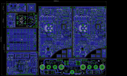
PCBs
... and PCBs (for closer inspection click on image and then on option "View image" on right mouse click menu)...
... and PCBs (for closer inspection click on image and then on option "View image" on right mouse click menu)...
Attachments
Last edited:
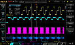
Few LM5118 pre-regulator measurements ...
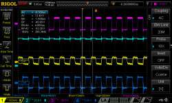
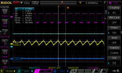
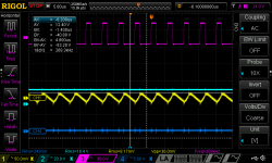
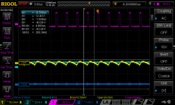
Here you can find some measurements done on pre-regulator (assembled on first PCB revision) with pure resistive load (two 8R2/100W in connected in series). Vin=40VAC therefore for the upper limit LM5118 is in buck-boost mode that generate more output ripple then is buck mode. For measurements are used simple short ground probing (no differential probing with two channels).
Channel color legend:
Yellow - Vout ripple (AC coupled)
Cyan - Vout (DC coupled)
Magenta - HI mosfet Gate
Blue - LO mosfet Gate
Power inductor is approx. 100uH (custom made on ETD29/16/10 ferrite core).
Attachments
-
 2014-12-27 PSU (design v0.30) Preg only, Vout=50V, Iout=3A, Load=16R4, Rramp=39K, Comp 100pF_8n2.png61.7 KB · Views: 287
 -
 2014-12-27 PSU (design v0.30) Preg only, Vout=41.2V, Iout=2.5A, Load=16R4, Rramp=39K, Comp 100pF.png51.9 KB · Views: 246
 -
 2014-12-27 PSU (design v0.30) Preg only, Vout=33.1V, Iout=2A, Load=16R4, Rramp=39K, Comp 100pF_8.png51.7 KB · Views: 233
 -
 2014-12-27 PSU (design v0.30) Preg only, Vout=24.6V, Iout=1.5A, Load=16R4, Rramp=39K, Comp 100pF.png53.8 KB · Views: 258
 -
 2014-12-27 PSU (design v0.30) Preg only, Vout=16.4V, Iout=1A, Load=16R4, Rramp=39K, Comp 100pF_8.png50.7 KB · Views: 365
 -
 2014-12-27 PSU (design v0.30) Preg only, Vout=8.4V, Iout=0.5A, Load=16R4, Rramp=39K, Comp 100pF_.png48.4 KB · Views: 474
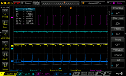
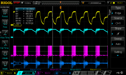
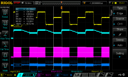
Step response using DAC programming ...
Additional possibly interesting measurement what I can provide in this moment is how PSU follow DAC instructions. Please note that measurement was performed with post-regulator section build on breadboard. DAC command was sent using Arduino in infinite loop sequence of three U_SET value each 5, 20 or 50ms long. Connected load was again 16R4 (2 x 8R2). As you can see there is no overshooting nor undershooting presents. Falling edge is possibly too slow. This is done with 100uF capacitor connected on the output. Channel color legend is the same as in the previous post. HI and LO gate signals frequency is too high to be seen correctly.
Additional possibly interesting measurement what I can provide in this moment is how PSU follow DAC instructions. Please note that measurement was performed with post-regulator section build on breadboard. DAC command was sent using Arduino in infinite loop sequence of three U_SET value each 5, 20 or 50ms long. Connected load was again 16R4 (2 x 8R2). As you can see there is no overshooting nor undershooting presents. Falling edge is possibly too slow. This is done with 100uF capacitor connected on the output. Channel color legend is the same as in the previous post. HI and LO gate signals frequency is too high to be seen correctly.
Attachments
-
 2015-01-02 PSU (design v0.31) with tracking, U_SET 0x05-0x30-0x55, 5-5-5ms.png62 KB · Views: 285
 -
 2015-01-02 PSU (design v0.31) with tracking, U_SET 0x05-0x30-0x55, 20-20-20ms.png60.5 KB · Views: 278
 -
 2015-01-02 PSU (design v0.31) with tracking, U_SET 0x05-0x30-0x55, 50-50-50ms.png49.6 KB · Views: 268
Very impressive and interesting! It is beyond my level of understanding (a little complex for my knowledge) but it looks as a top of the range PSU.
Looking forward for further progress.
BTW, you chose a high voltage level (50V) but you limit the current to only 3A, I think a higher current level would be more useful in a dual PS, in order to serve power amps' test for example.
Looking forward for further progress.
BTW, you chose a high voltage level (50V) but you limit the current to only 3A, I think a higher current level would be more useful in a dual PS, in order to serve power amps' test for example.
Very impressive and interesting! It is beyond my level of understanding (a little complex for my knowledge) but it looks as a top of the range PSU.
Looking forward for further progress.
BTW, you chose a high voltage level (50V) but you limit the current to only 3A, I think a higher current level would be more useful in a dual PS, in order to serve power amps' test for example.
Thanks Spiritos. Actually it looks a little bit scary on the first sight due to the digital part and binding post section (which is really an extra luxury). The core is actually presented on the Sheet 2 with "preparation" done on Sheet 1 where you can see SMPS pre-regulator and bias power supply. Yes, that two guys looks unnecessary complex but offer a promise to works with various input transformer thanks to buck-boost topology and LM5118 is doing a really great job. Ok, maybe that is meaningless for the final product but in this testing phase it helps me to learn a bit about SMPS stuff.
If we stay strictly within buck region (Vin > Vout) with selected bias supply (low noise in 200KHz region LDO's as post-regulators) and N-ch MOSFET based main post-regulator which is very quiet it could be possible to ends up with Vout noise level acceptable for audio testing (due to that it was also highly on the list of requirements a no cooling fan solution to not kill a joy of listening performance of a connected preamp or smaller amp stage).
I'm agree that 3A is really not enough for some bigger amps testing but what I can preliminary say that it should reach easily 5A with proper transformer and MOSFET even with max Vout of 50V. Also don't forget that the project goal is dual channel unit with possibility for serial or parallel connection. The former gives you 0-100V range and the latest 6A (or hopefully 10A).
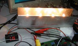
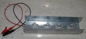
While waiting for PCBs I spent some time to organize my halogen lamps based dummy load in a proper way (holder of the first one was almost melted by high temperature). Here are some pictures if some find such approach useful. Ceramic lamp holder is HE01-150.
Attachments

Front panel design excercise
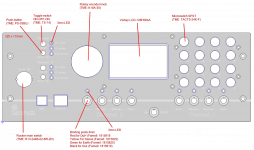
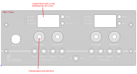
I spent some time to test how is working Front Panel Designer (v4.41 for 64-bit linux) from Schaeffer AG. It's really nice and simple tool covering everything that I can imagine in this moment. Great feature is built-in price calculator. Unfortunately not so nice "feature" is the total cost of simple design . Here is what I have in mind for MCU controlled and manually controlled dual channel unit. I took as a reference dimensions of Modushop's Alu-cases (with front panel's of 320x115mm and 280x115mm respectively).
The first design costs 73.91EUR (87.95EUR incl. VAT, excl. S&H) and the second one 109.74EUR (130.59EUR incl. VAT, excl. S&H) 😱. Does anybody recently made an order that can tell me how accurate is that price calculator?
I spent some time to test how is working Front Panel Designer (v4.41 for 64-bit linux) from Schaeffer AG. It's really nice and simple tool covering everything that I can imagine in this moment. Great feature is built-in price calculator. Unfortunately not so nice "feature" is the total cost of simple design
. Here is what I have in mind for MCU controlled and manually controlled dual channel unit. I took as a reference dimensions of Modushop's Alu-cases (with front panel's of 320x115mm and 280x115mm respectively). The first design costs 73.91EUR (87.95EUR incl. VAT, excl. S&H) and the second one 109.74EUR (130.59EUR incl. VAT, excl. S&H) 😱. Does anybody recently made an order that can tell me how accurate is that price calculator?
Attachments
100% accurate (excluding shipping costs back and forth if needed, of course).
They charge you based on the sum calculated by their app.
They charge you based on the sum calculated by their app.
Thanks for your input. I'll possibly take another route using thiner Alu plate (1.5-2mm) make all holes by myself and find some cheaper laser engraving or color transfer method for labels.
Of course any new idea is welcomed.
Of course any new idea is welcomed.
wow - nice project. There are some cool diy ideas for front panels.
A couple -
Professional looking front panels
FRONT PANEL DESIGN AND CONSTRUCTION IN SYNTHESIZER PROJECTS
A couple -
Professional looking front panels
FRONT PANEL DESIGN AND CONSTRUCTION IN SYNTHESIZER PROJECTS
Excellent recommendations! I like this Lazertran solution (Method 3 from FRONT PANEL CONSTRUCTION IN SYNTHESIZER PROJECTS), but also polypropylene (PP) folder approach (described in Professional looking front panels) has a great feature to make "windows" which can make LED's position very attractive. Many thanks!
The following approach was recommended by a forum member in another thread:
https://www.youtube.com/watch?v=Yj0Bv4UEFSs
I think you'll find it interesting. 🙂
https://www.youtube.com/watch?v=Yj0Bv4UEFSs
I think you'll find it interesting. 🙂
The following approach was recommended by a forum member in another thread:
https://www.youtube.com/watch?v=Yj0Bv4UEFSs
I think you'll find it interesting. 🙂
Fantastic idea! Huh, how many hours I spent working on PCB layout without idea that it can be used for other important part of the project 😱
I agree with you prasimix, I ask me why i don't have think about that before !
As of you, i will seriously look this solution for my own psu project.
And also very good work for your project ! 🙂
Frex
As of you, i will seriously look this solution for my own psu project.
And also very good work for your project ! 🙂
Frex
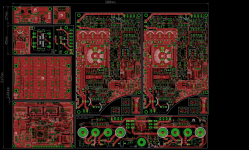
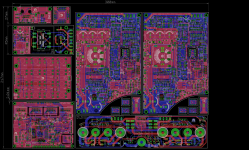
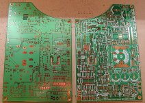
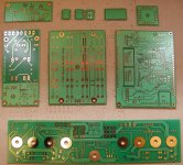
PCBs is arrived...
PCB's arrived yesterday or within 2 weeks from moment of ordering. A nice supplier (printed.cz) which I'd like to recommend (thanks permaneder).
Here is the main board where is located all circuit from Sheet 1 to 4 namely input bridge rectifier and capacitors, power pre-regulator, power post-regulator (CV and CC), bias supply pre-regulator and LDOs, OCP, CC/CV indicators and isolated sync for pre-regulators. That is a functional analog part of the PSU. On the same board is also located digital part that is used to communicate with MCU board via SPI. That mean DAC, ADC and I/O expander.
Attachments

Nice PCB Job. Where can we buy ?
🙂 Not so soon but shortly after I finalized testing of all functionality and make additional optimization and hopefully decrease number of components where possible. My intention is to first make functional, robust and stable power board which can be controlled manually (using pots and switches) and after that we can continue to play with MCU and Arduino-like code in case of the presented MCU board. Of course any suggestion regarding current design is highly welcomed.
- Home
- Design & Build
- Equipment & Tools
- DIY programmable dual channel bench PSU 0-50V/3A