Thank you for sharing.
I have one question, what happens at the ouput terminals at switch on / off the supply?
Fex when using only manual control.
I have one question, what happens at the ouput terminals at switch on / off the supply?
Fex when using only manual control.
Thank you for sharing.
I have one question, what happens at the ouput terminals at switch on / off the supply?
Fex when using only manual control.
Don't know what fex means 😕 but if you asking about possible overshooting it is not present. In current design I added timer with relay to add power up delay and also power down cut off (Q4 gate is grounded). All this is tested with separate linear bias power supply (LM317/337) when on power down bias supply went out too early that Q4 control is lost what caused that remaining voltage from input capacitors (C12, C13) is present on the output (similar problem was with power up). With a new bias power supply which include SMPS pre-regulator IC3, and LDO'2 IC2 and IC4 and using Powergood signal to enable/start the main pre-regulator (IC1) possibly a timer+relay circuit will be redundant.
Good to knowFex is swenglish (swedish + englsh) for example 🙂

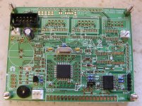
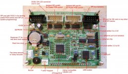
MCU board assembled ...
I know that this is not a correct order of presenting what is already done under PSU project but I didn't have a chance to make a lot of progress on power board (I got yesterday required inductor for bias ps) so I decide to test how MCU board is working.
The following pictures shows MCU board with minimum components required to make connection to ISP programmer (I'm using Arduino for that) and run simple test melody on buzzer. I reused the following code:
... and required header file:
I know that this is not a correct order of presenting what is already done under PSU project but I didn't have a chance to make a lot of progress on power board (I got yesterday required inductor for bias ps) so I decide to test how MCU board is working.
The following pictures shows MCU board with minimum components required to make connection to ISP programmer (I'm using Arduino for that) and run simple test melody on buzzer. I reused the following code:
Code:
/*
 Melody

 Plays a melody

 created 21 Jan 2010
 modified 30 Aug 2011
 by Tom Igoe

This example code is in the public domain.

 http://arduino.cc/en/Tutorial/Tone

*/

#include "pitches.h"

// notes in the melody:
int melody[] = {
  NOTE_C4, NOTE_G3,NOTE_G3, NOTE_A3, NOTE_G3,0, NOTE_B3, NOTE_C4};

// note durations: 4 = quarter note, 8 = eighth note, etc.:
int noteDurations[] = {
  4, 8, 8, 4,4,4,4,4 };

void setup() {
  // iterate over the notes of the melody:
  for (int thisNote = 0; thisNote < 8; thisNote++) {

    // to calculate the note duration, take one second
    // divided by the note type.
    //e.g. quarter note = 1000 / 4, eighth note = 1000/8, etc.
    int noteDuration = 1000/noteDurations[thisNote];
    tone(A1, melody[thisNote],noteDuration); // Arduino pin A1 is PF6 (Pin 37) assigned to BUZZER

    // to distinguish the notes, set a minimum time between them.
    // the note's duration + 30% seems to work well:
    int pauseBetweenNotes = noteDuration * 1.30;
    delay(pauseBetweenNotes);
    // stop the tone playing:
    noTone(A1);
  }
}

void loop() {
  // no need to repeat the melody.
}
... and required header file:
Code:
/*************************************************
 * Public Constants
 *************************************************/

#define NOTE_B0  31
#define NOTE_C1  33
#define NOTE_CS1 35
#define NOTE_D1  37
#define NOTE_DS1 39
#define NOTE_E1  41
#define NOTE_F1  44
#define NOTE_FS1 46
#define NOTE_G1  49
#define NOTE_GS1 52
#define NOTE_A1  55
#define NOTE_AS1 58
#define NOTE_B1  62
#define NOTE_C2  65
#define NOTE_CS2 69
#define NOTE_D2  73
#define NOTE_DS2 78
#define NOTE_E2  82
#define NOTE_F2  87
#define NOTE_FS2 93
#define NOTE_G2  98
#define NOTE_GS2 104
#define NOTE_A2  110
#define NOTE_AS2 117
#define NOTE_B2  123
#define NOTE_C3  131
#define NOTE_CS3 139
#define NOTE_D3  147
#define NOTE_DS3 156
#define NOTE_E3  165
#define NOTE_F3  175
#define NOTE_FS3 185
#define NOTE_G3  196
#define NOTE_GS3 208
#define NOTE_A3  220
#define NOTE_AS3 233
#define NOTE_B3  247
#define NOTE_C4  262
#define NOTE_CS4 277
#define NOTE_D4  294
#define NOTE_DS4 311
#define NOTE_E4  330
#define NOTE_F4  349
#define NOTE_FS4 370
#define NOTE_G4  392
#define NOTE_GS4 415
#define NOTE_A4  440
#define NOTE_AS4 466
#define NOTE_B4  494
#define NOTE_C5  523
#define NOTE_CS5 554
#define NOTE_D5  587
#define NOTE_DS5 622
#define NOTE_E5  659
#define NOTE_F5  698
#define NOTE_FS5 740
#define NOTE_G5  784
#define NOTE_GS5 831
#define NOTE_A5  880
#define NOTE_AS5 932
#define NOTE_B5  988
#define NOTE_C6  1047
#define NOTE_CS6 1109
#define NOTE_D6  1175
#define NOTE_DS6 1245
#define NOTE_E6  1319
#define NOTE_F6  1397
#define NOTE_FS6 1480
#define NOTE_G6  1568
#define NOTE_GS6 1661
#define NOTE_A6  1760
#define NOTE_AS6 1865
#define NOTE_B6  1976
#define NOTE_C7  2093
#define NOTE_CS7 2217
#define NOTE_D7  2349
#define NOTE_DS7 2489
#define NOTE_E7  2637
#define NOTE_F7  2794
#define NOTE_FS7 2960
#define NOTE_G7  3136
#define NOTE_GS7 3322
#define NOTE_A7  3520
#define NOTE_AS7 3729
#define NOTE_B7  3951
#define NOTE_C8  4186
#define NOTE_CS8 4435
#define NOTE_D8  4699
#define NOTE_DS8 4978
Attachments
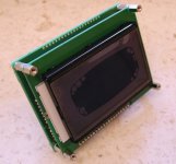
LCD display on the MCU board ...
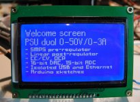
... and some pictures where a fully assembled board with connected LCD 128x64 and test message (using u8glib) is showed. Here is the code:
... and some pictures where a fully assembled board with connected LCD 128x64 and test message (using u8glib) is showed. Here is the code:
Code:
#include "U8glib.h" // Universal 8bit Graphics Library, http://code.google.com/p/u8glib/

// Define LCD type
// devices with all constructor calls is here: http://code.google.com/p/u8glib/wiki/device
U8GLIB_ST7920_128X64_1X u8g(A0); // Arduino Pin A0 is PF7 (pin 36) assigned to LCD_SELECT

void draw(void) {
  // graphic commands to redraw the complete screen should be placed here
  //u8g.setFont(u8g_font_unifont);
  u8g.setFont(u8g_font_tpss);
  //u8g.setFont(u8g_font_osb21);
  //u8g.setFont(u8g_font_04b_03b);
  u8g.drawStr( 0, 10, "Welcome screen");
  u8g.drawStr( 0, 22, "PSU dual 0-50V/0-3A");
  u8g.setFont(u8g_font_04b_03b);
  u8g.drawStr( 0, 30, "- SMPS pre-regulator");
  u8g.drawStr( 0, 36, "- Linear post-regulator");
  u8g.drawStr( 0, 42, "- CC/CV, OCP");
  u8g.drawStr( 0, 48, "- 16-bit DAC, 15-bit ADC");
  u8g.drawStr( 0, 54, "- Isolated USB and Ethernet");
  u8g.drawStr( 0, 60, "- Arduino sketches");
}

void setup(void) {
  // Set LCD brightness
  pinMode(11, OUTPUT); // Arduino Pin 11 is PB7 (pin 12) assigned to LCD_BRIGHTNESS
  analogWrite(11, 200); // (value from 0 to 255, 0=dark)

  if ( u8g.getMode() == U8G_MODE_R3G3B2 ) {
    u8g.setColorIndex(255);     // white
  }
  else if ( u8g.getMode() == U8G_MODE_GRAY2BIT ) {
    u8g.setColorIndex(3);         // max intensity
  }
  else if ( u8g.getMode() == U8G_MODE_BW ) {
    u8g.setColorIndex(1);         // pixel on
  }
  else if ( u8g.getMode() == U8G_MODE_HICOLOR ) {
    u8g.setHiColorByRGB(255,255,255);
  }

  u8g.firstPage();
  do {
    draw();
  } while( u8g.nextPage() );
}

void loop(void) {

  // Nothing to do

}
Attachments
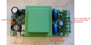
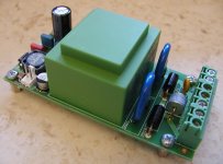
Aux power supply
Aux power supply PCB is assembled and tested. LM5574 works nicely and I choose it because it is also used for bias power supply on power board when input voltage could go up to 67V. The board is intended to provide separated +5V for MCU board and Binding posts board. Max. consumption is ~400mA (mostly consumed by binding posts LEDs and relays when all are active) which LM5574 is delivering without problem.
Here are some pictures of assembled board and basic measurements.
Attachments
-
 2015-02-11 Aux power supply power up and down (full load 370mA).png31.4 KB · Views: 217
 -
 2015-02-12 Aux power supply transient response (full load 370mA).png40.5 KB · Views: 224
 -
 2015-02-11 Aux power supply output ripple + sync (20MHz).png46.3 KB · Views: 284
 -
 Aux power supply (2).JPG402.4 KB · Views: 313
 -
 Aux power supply.JPG357.4 KB · Views: 565
your project is superb. i am a hobbyist from India. I think it is a big project for an average hobbyist like me . Please post a version with manual controls only.
your project is superb. i am a hobbyist from India. I think it is a big project for an average hobbyist like me . Please post a version with manual controls only.
For manual controls version you need circuits presents on sheets 1 to 3 and simply ignore the rest. For that you need only PCB presented in #17 (partially populated since it contains also Sheet 4 circuits). Also I think that further simplification is possible on the first three sheets i.e. I'll possibly replace current buck-boost pre-regulator built around LM5118 with buck using LM5088. Also bias power supply with LT3030 and TPS7A3001 could be done with simpler and cheaper components. It's still a work in progress and I'll present such derivatives in this or new thread.
Just one remark regarding LM5118: on the first sight it looks like an overkill but it opens a whole new possibility to use car battery (12V) or even solar panel on input instead of main transformer and then it starts to make much more sense. Of course boost mode is more noisy and require bigger components because currents could be a few times higher if we'd like to deliver a full monty (up to 50V, and 3A). But if working in boost mode is limited to i.e. 50W (instead of 150W) then I think it should be achievable without bigger modifications.
I don't know if possibility to source a PSU from car battery or solar panel make a lots of sense because with that we are leaving bench and become portable so I hope that I'll also get some feedback from forum members over the time what route is more desirable: "buck-boost" or "buck" only.
Power pre-regulator inital testing
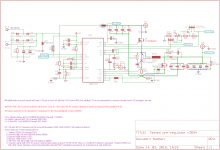
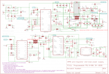
Power pre-regulator is located on the power PCB (post #17) and initially presented on the Sheet 1 (post #2). I'd like to share some information about initial testing of this part of the system.
First I'd like to starts with some mistakes. Input filter capacitors are located optimistically too close to the rectifier diodes D2 and D3. Since that diodes has to be mounted with screw to the main heatsink there is not many spaces for maneuvering with a screwdriver. It's so difficult to mount mentioned diodes but they could be more accessible.
Another mistake that cost me one LM5118 is that I forgot to add a small resistor in serial with P1. In normal operation a whole section P1, R1 and R2 is not necessary since PREG_FB signal (Sheet 2) will be used for controlling PREG_OUT. I added this section deliberately because in that way you can assemble and test power pre-regulator section without tracking control and the rest of the post-regulator (Sheet 2). So what's happened? P1 was initially set for Vout below 10V and I started to turn P1 too fast (approaching ground) and since LM5118 is buck-boost controller it has no problem to increase Vout to 100V! I heard click and the next action was removing LM5118 with rose's metal from the PCB and mounting another one .
.
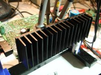
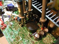
In attachment you can see pre-regulator section of the power PCB. Power inductor (TR1) is Wishay IHTH1125MZEB101M5A. Selected heatsink is RAD-A52317/50 (painted in black). I'll play in the future with other inductors and try heatsink Fischer SK85/50/SA.
Currently I've measured the following temperatures on some key components under max. load when LM5118 enters buck-boost mode (@Iout=3A, Vin=48VAC, Load=16R4, Tabient=23oC):
Power pre-regulator is located on the power PCB (post #17) and initially presented on the Sheet 1 (post #2). I'd like to share some information about initial testing of this part of the system.
First I'd like to starts with some mistakes. Input filter capacitors are located optimistically too close to the rectifier diodes D2 and D3. Since that diodes has to be mounted with screw to the main heatsink there is not many spaces for maneuvering with a screwdriver. It's so difficult to mount mentioned diodes but they could be more accessible.
Another mistake that cost me one LM5118 is that I forgot to add a small resistor in serial with P1. In normal operation a whole section P1, R1 and R2 is not necessary since PREG_FB signal (Sheet 2) will be used for controlling PREG_OUT. I added this section deliberately because in that way you can assemble and test power pre-regulator section without tracking control and the rest of the post-regulator (Sheet 2). So what's happened? P1 was initially set for Vout below 10V and I started to turn P1 too fast (approaching ground) and since LM5118 is buck-boost controller it has no problem to increase Vout to 100V! I heard click and the next action was removing LM5118 with rose's metal from the PCB and mounting another one
.In attachment you can see pre-regulator section of the power PCB. Power inductor (TR1) is Wishay IHTH1125MZEB101M5A. Selected heatsink is RAD-A52317/50 (painted in black). I'll play in the future with other inductors and try heatsink Fischer SK85/50/SA.
Currently I've measured the following temperatures on some key components under max. load when LM5118 enters buck-boost mode (@Iout=3A, Vin=48VAC, Load=16R4, Tabient=23oC):
- Rsense (R12): 72oC
- TR1: 53oC
- L1: 51oC
- Cout (3x180uF): 51oC
- Cin (1x2200uf): 44oC
- Heatsink: 56oC
- Rsense (R12): 46oC
- TR1: 32oC
- L1: 51oC
- Cout (3x180uF): 31oC
- Cin (1x2200uf): 30oC
- Heatsink: 34oC
Attachments
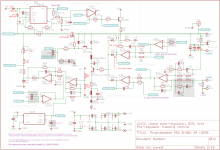
Schematic of tested power preregulator and measurements ...
Attached schematic reflects changes added to the initial version of the power pre-regulator presented in Sheet 1 (post #2). It's accompanied with my version of TI's quick calculator that is used for defining component's value.
Unfortunately I didn't succeed with deployment of the output filter (L2, L3, C17 in the first version from post #2) to further decrease ripple without serious oscillations when load is attached so it's for now removed from the schematic.
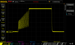
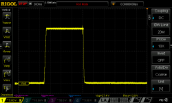
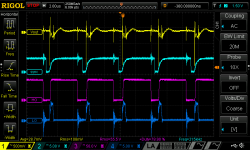
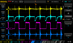
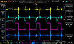
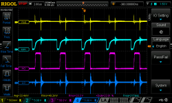
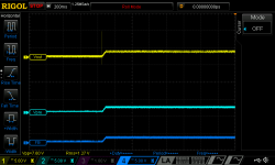
For testing I've used various resistive loads incl. lamps (see post #8, which actually works like a huge PTC resistor) and DC motor as an inductive load. Signal traces are marked with Vout, Sync (LM5118's pin 11), HO (pin 19) and LO (pin 15). I tried to checked output ripple, possible instability with various loads, gate output signal and power up/down overshoot. I hope that picture titles are self-explaining and as you can see I went with testing Iout with up to 5A (ok, still within projected 150W).
Interesting and on the first sight possibly misleading picture is one which shows power up and down with 4x35W lamp load connected. Since when lamp is cold its resistance is similar to short circuit, LM5118 gradually reach required Vout as wire filament heated.
Attached schematic reflects changes added to the initial version of the power pre-regulator presented in Sheet 1 (post #2). It's accompanied with my version of TI's quick calculator that is used for defining component's value.
Unfortunately I didn't succeed with deployment of the output filter (L2, L3, C17 in the first version from post #2) to further decrease ripple without serious oscillations when load is attached so it's for now removed from the schematic.
For testing I've used various resistive loads incl. lamps (see post #8, which actually works like a huge PTC resistor) and DC motor as an inductive load. Signal traces are marked with Vout, Sync (LM5118's pin 11), HO (pin 19) and LO (pin 15). I tried to checked output ripple, possible instability with various loads, gate output signal and power up/down overshoot. I hope that picture titles are self-explaining and as you can see I went with testing Iout with up to 5A (ok, still within projected 150W).
Interesting and on the first sight possibly misleading picture is one which shows power up and down with 4x35W lamp load connected. Since when lamp is cold its resistance is similar to short circuit, LM5118 gradually reach required Vout as wire filament heated.
Attachments
-
snvu065a for PSU pre-regulator.ods.zip192.6 KB · Views: 230
-
 2015-02-14 Pre-regulator Vin=48VAC, Vout=25V, Load=4x35W lamp, Iout=3A, power up and down.png38.7 KB · Views: 215
 -
 2015-02-14 Pre-regulator Vin=48VAC, Vout=25V, Load=8R2, Iout=3A, power up and down.png38.2 KB · Views: 174
 -
 2015-02-14 Pre-regulator Vin=48VAC, Load=DC motor, Vout=12V, Iout=1A.png46.5 KB · Views: 663
 -
 2015-02-13 Pre-regulator Vin=48VAC, Load=4x35W lamp, Vout=48V, Iout=3A.png56.4 KB · Views: 694
 -
 2015-02-14 Pre-regulator Vin=48VAC, Load=4R1, Vout=21V, Iout=5A.png58.6 KB · Views: 706
 -
 2015-02-14 Pre-regulator Vin=48VAC, Load=4R1, Vout=17V, Iout=4A.png52.7 KB · Views: 745
 -
 2015-02-14 Pre-regulator Vin=48VAC, Load=4R1, Vout=13V, Iout=3A.png50.2 KB · Views: 798
 -
 Tested pre-regulator r2B34.png63.1 KB · Views: 444
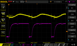
Power pre-regulator efficiency...
I tried to get some idea about power dissipation and does current heatsink will be enough for extreme case (50V/3A on output). Measuring Vin and Iin as AC (rms) and Vout and Iout as DC I got the following data:
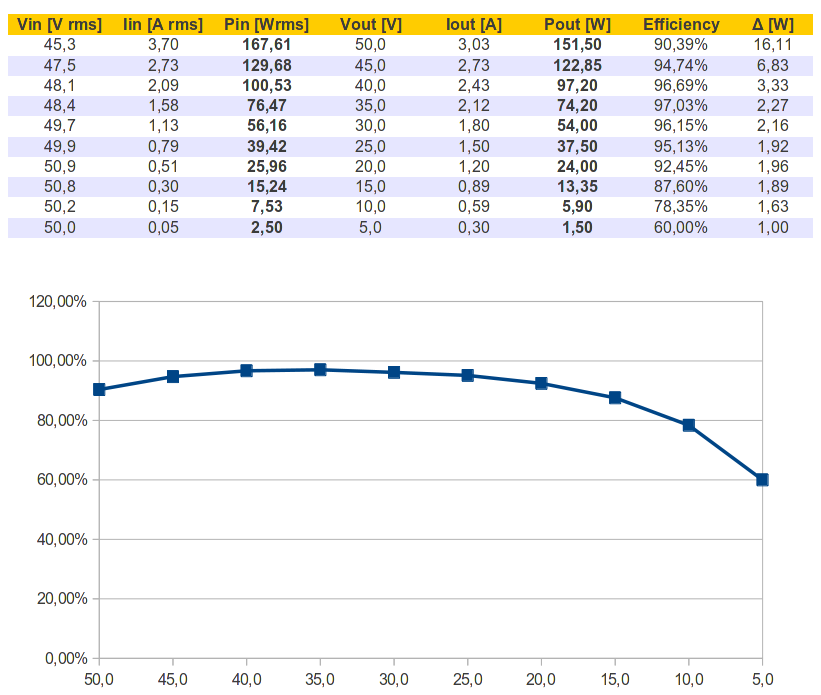
If I substract few Watts from ~16W in 50/3A that is dissipated on power inductor (TR1) and Rsense (R12), and also add a couple of Watts because I have to go up to 52V/3A plus at least 6W on Q4 from post-regulator then it's still ~20W for max. output. Due to that probably a little bit bigger heatsink will be required. A previously suggested SK85/50/SA with thermal resistance Rth od 1.35K/W should do a good job keeping temperature to the 50oC if Tambient is 23oC.
I tried to get some idea about power dissipation and does current heatsink will be enough for extreme case (50V/3A on output). Measuring Vin and Iin as AC (rms) and Vout and Iout as DC I got the following data:
If I substract few Watts from ~16W in 50/3A that is dissipated on power inductor (TR1) and Rsense (R12), and also add a couple of Watts because I have to go up to 52V/3A plus at least 6W on Q4 from post-regulator then it's still ~20W for max. output. Due to that probably a little bit bigger heatsink will be required. A previously suggested SK85/50/SA with thermal resistance Rth od 1.35K/W should do a good job keeping temperature to the 50oC if Tambient is 23oC.
Attachments
Doubt about installing heatsink on the back panel of Alu-enclosure
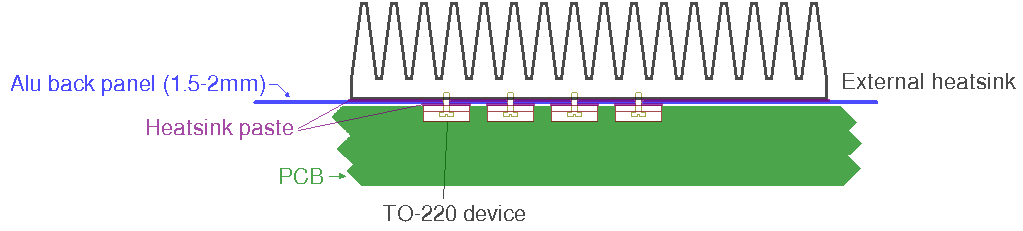
I have doubts about one rather simple issue: how to install heatsink on back panel of Alu-enclosure in the most efficient way? When I say efficient mean thermally and financially. One possibility is to open a huge rectangular hole on back panel that all TO-220 devices can be mounted directly on to heatsink. Another one is to mount them directly to the back panel and mount heatsink on opposite (external) side to assist thermal conduction. Second option is mechanically simpler (and cheaper) but with possibly lower thermal performance. But how much lower? Is it worth considering such option? Back panel area will be 280x115mm or 320x115mm (1.5-2mm thick). I'm not aware of calculator which take into account such setup.
I have doubts about one rather simple issue: how to install heatsink on back panel of Alu-enclosure in the most efficient way? When I say efficient mean thermally and financially. One possibility is to open a huge rectangular hole on back panel that all TO-220 devices can be mounted directly on to heatsink. Another one is to mount them directly to the back panel and mount heatsink on opposite (external) side to assist thermal conduction. Second option is mechanically simpler (and cheaper) but with possibly lower thermal performance. But how much lower? Is it worth considering such option? Back panel area will be 280x115mm or 320x115mm (1.5-2mm thick). I'm not aware of calculator which take into account such setup.
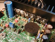
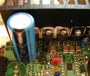
Power board update...
Power board is completely assembled and main function was tested. I have some good and some not so good and some bad news. Let's start with good one. Using bias power supply presented on the Sheet1 works much better and power up and down issues with overshooting caused by improper power sequencing is not exists any more. While "breadboarding" I used external transformer and set of standard linear regulators (7815, 7805, LM337) that provides required +15, +5 and -15V too late during power-up and vanish too early when power goes down. Power up and down sequencing can be found in the attachment. As a result a whole "mechanic" about controlling post-requlator power mosfet bias with TLC555 and relay is not necessary anymore freeing some PCB real estate.
Not so good news is that I found a mistake in connecting bias power supply coupled inductor. Fortunately it's not so big and with a couple of track cut and rewiring it works fine with existing PCB layout. A new Sheet1 with corrected coupled inductor wiring is also attached. LM5574 works very nicely alone and selected LDO's is probably overkill for DIY project. I'll probably in next PCB layout make a space for lower-cost alternative like LM317, LM1117 and LM337.
Finally a bad news. Currently the only "small detail" which stopping me to announce this board finished is that planned tracking control does works with LM5118. It even ends up with its blowout wiping out my LM5118 stock like a storm . So, LM5118 works just perfectly when it is controlled with "standard" feedback derived from resistor divider network (R1/P1, R2 from the latest Sheet1). When JP2 is shorted on position 1-2 I have a real mess. It even cause that ZD1 used to connect Vccx to the aux bias (as a mean of lowering LM5118 dissipation) is destroyed! I hope that TI's people will came up with some ideas or completely different approach will be required (based on simple PNP or optocoupler trackers published in some LTC's application notes).
Power board is completely assembled and main function was tested. I have some good and some not so good and some bad news. Let's start with good one. Using bias power supply presented on the Sheet1 works much better and power up and down issues with overshooting caused by improper power sequencing is not exists any more. While "breadboarding" I used external transformer and set of standard linear regulators (7815, 7805, LM337) that provides required +15, +5 and -15V too late during power-up and vanish too early when power goes down. Power up and down sequencing can be found in the attachment. As a result a whole "mechanic" about controlling post-requlator power mosfet bias with TLC555 and relay is not necessary anymore freeing some PCB real estate.
Not so good news is that I found a mistake in connecting bias power supply coupled inductor. Fortunately it's not so big and with a couple of track cut and rewiring it works fine with existing PCB layout. A new Sheet1 with corrected coupled inductor wiring is also attached. LM5574 works very nicely alone and selected LDO's is probably overkill for DIY project. I'll probably in next PCB layout make a space for lower-cost alternative like LM317, LM1117 and LM337.
Finally a bad news. Currently the only "small detail" which stopping me to announce this board finished is that planned tracking control does works with LM5118. It even ends up with its blowout wiping out my LM5118 stock like a storm
. So, LM5118 works just perfectly when it is controlled with "standard" feedback derived from resistor divider network (R1/P1, R2 from the latest Sheet1). When JP2 is shorted on position 1-2 I have a real mess. It even cause that ZD1 used to connect Vccx to the aux bias (as a mean of lowering LM5118 dissipation) is destroyed! I hope that TI's people will came up with some ideas or completely different approach will be required (based on simple PNP or optocoupler trackers published in some LTC's application notes).Attachments
Last edited:
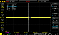
I made some progress playing with tracking control for pre-regulator. To be sure and avoid destruction of new arrived LM5118s first I tested that everything works replacing the lower resistor with a LDR (Farnell: 2293503) in resistor divider based feedback to set pre-regulator Vout (or PREG_OUT in schematic). After that step I built a tracking control coupling LDR with 3mm red LED which could be replaced in the final stage with some ready made solution (i.e. NSL-32SR3, Farnell: 3692218).
This solution works providing difference of ~2.1V between PREG_OUT and OUT+ (after post-regulator), but not completely. It failed to set a desired voltage if during power up load is connected (i.e. 100R resistor) 🙁.
If load is connected after power up everything continue to work fine: pre-regulator is "locked" to post-regulator output. Currently don't have idea why is that and yours suggestions are welcomed. Please also find in attachment some measurements during power up: without load (set Vout=10V), without load (set Vout=18V) and with 100R load (set Vout=10V or any other higher then 1.2V).
Please note that "glitch" when Vout is set to 10V. It's present for Vout range of approx. 2v to 18V. Maybe that's a clue to the workable solution 😕. Is it in any way connected with the fact that power mosfet driver is not connected to ground but to -2V currently derived from -15V using 13V Zener diode?
Attachments
-
 2015-03-06 LED-LDR Tracking control, Vout=1.2V (set to 10V), L=100R.png35 KB · Views: 156
 -
 2015-03-06 LED-LDR Tracking control, Vout=18V, no load.png38.4 KB · Views: 185
 -
 2015-03-06 LED-LDR Tracking control, Vout=10V, no load (2).png46.3 KB · Views: 239
 -
 LDR-LED tracking control.png14.6 KB · Views: 334
regarding mounting semiconductors, I strongly suggest you cut a hole in the back wall.
Otherwise you need to use extensive screwing to prevent air gaps between the wall and heatsink, as the former probably will warp. Any rigid metallic object between semiconductor surface and heatsink will cause small airgaps.
Regarding your troubles with blowing up the buck regulator, I have justed looked quickly at your schematic but are you shure you are not driving the inputs at to high potential, ie you need some isolated transfer , fex optocoupler as you suggest.
regarding mounting semiconductors, I strongly suggest you cut a hole in the back wall.
Otherwise you need to use extensive screwing to prevent air gaps between the wall and heatsink, as the former probably will warp. Any rigid metallic object between semiconductor surface and heatsink will cause small airgaps.
Thanks for your feedback. Do you think that applying heatsink paste cannot "fill the gaps" even if we have here two areas (both side of chassis back panel)?
Regarding your troubles with blowing up the buck regulator, I have justed looked quickly at your schematic but are you shure you are not driving the inputs at to high potential, ie you need some isolated transfer , fex optocoupler as you suggest.
I blew up few od them when I played with inital "complex" tracking control that is on the PCB. It works fine if simple resistor divider is used or LDR-LED optocoupling described in my previous post.
Attachments

I think that to get sufficient contact between to 220 capsule , back wall and heatsink ypu might damage the to 220 due to the high torque/ pressure necessary.
The heatsink paste should not be more than say a houndred microns thick, no more to bridge the airgaps between the uneven surfaces. It is like putting two handsaw blades teeth against teeth, the paste should fill the void in between.
The heatsink paste should not be more than say a houndred microns thick, no more to bridge the airgaps between the uneven surfaces. It is like putting two handsaw blades teeth against teeth, the paste should fill the void in between.
Current status...
Many things have happened since my last post. I continued my quest for workable tracking control and tried one that is e.g. used in LTC’s DC2132A. It’s interesting that they have two schematic revision where tracking control section is updated. Both of them contains RC filter without values. Don’t know why possibly because a whole thing is not so exact and require some experimenting. I tried that circuit and can say that it works fine up to ~25V and after that it starts to produce instability in SMPS pre-regulator especially after 30V which makes this solution unacceptable for my project. I tried to isolate PNP from FB pin using regular optocoupler (4N35), it works a little bit better but still not acceptable and finally when I used LDR coupled with LED it works nice up to 50V. So lets say that this part of the story is closed.
After that I decide to test NSB Lab design presented here and here. Finally I started to use spice software, first Simetrix but shortly came to free version limitation 🙁. That’s pity since this software works really nice and I started to use it almost instantly. Anyway simple CV control loop model for Simetrix is enclosed in attachment.
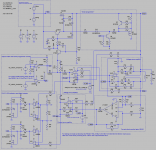
Next station was LTspice. Thanks to massive and excellent assistance from Leonid (NSB Lab) I ended up with model which is also enclosed. Actually three of them. First is with LTC2057 as a current shunt monitor which I selected since I have few of them on disposal for breadboarding.
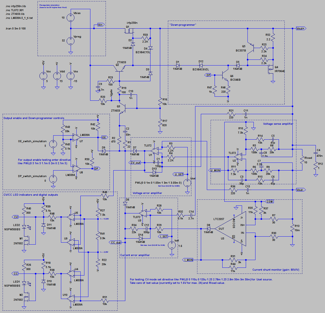
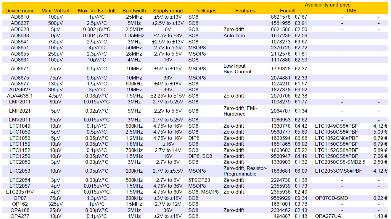
Second model is derived from previous one as an example of CV control loop only in case that you have the same problem that I noticed – simulation lasts possibly forever (I left it overnight but without success). It’s possibly a problem with my environment since I’m running LTspice on Ubuntu with Wine. Due to that I also send in attachment another model with AD8610 used as current shunt monitor. I currently have no plan to test AD8610 since it doesn’t look attractive due to its high price. Final candidate for this function is still not selected, but there is no need to stick with only one since there is many nice op-amps that can be used. Here is the table with some of them that I found interesting.
Any your inputs is highly welcomed. In the final step when a new PCB has to be made I need to decide which package to use SO8 or MSOP8. Again, your inputs is welcomed.
Many things have happened since my last post. I continued my quest for workable tracking control and tried one that is e.g. used in LTC’s DC2132A. It’s interesting that they have two schematic revision where tracking control section is updated. Both of them contains RC filter without values. Don’t know why possibly because a whole thing is not so exact and require some experimenting. I tried that circuit and can say that it works fine up to ~25V and after that it starts to produce instability in SMPS pre-regulator especially after 30V which makes this solution unacceptable for my project. I tried to isolate PNP from FB pin using regular optocoupler (4N35), it works a little bit better but still not acceptable and finally when I used LDR coupled with LED it works nice up to 50V. So lets say that this part of the story is closed.
After that I decide to test NSB Lab design presented here and here. Finally I started to use spice software, first Simetrix but shortly came to free version limitation 🙁. That’s pity since this software works really nice and I started to use it almost instantly. Anyway simple CV control loop model for Simetrix is enclosed in attachment.
Next station was LTspice. Thanks to massive and excellent assistance from Leonid (NSB Lab) I ended up with model which is also enclosed. Actually three of them. First is with LTC2057 as a current shunt monitor which I selected since I have few of them on disposal for breadboarding.
Second model is derived from previous one as an example of CV control loop only in case that you have the same problem that I noticed – simulation lasts possibly forever (I left it overnight but without success). It’s possibly a problem with my environment since I’m running LTspice on Ubuntu with Wine. Due to that I also send in attachment another model with AD8610 used as current shunt monitor. I currently have no plan to test AD8610 since it doesn’t look attractive due to its high price. Final candidate for this function is still not selected, but there is no need to stick with only one since there is many nice op-amps that can be used. Here is the table with some of them that I found interesting.
Any your inputs is highly welcomed. In the final step when a new PCB has to be made I need to decide which package to use SO8 or MSOP8. Again, your inputs is welcomed.
Attachments
Last edited:
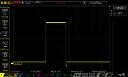
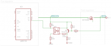
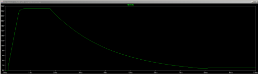
Down-programmer...
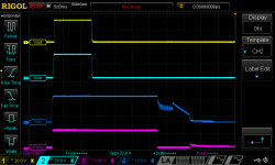
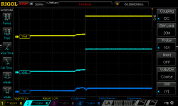
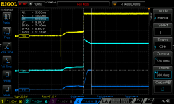
New post-regulator include so-called down-programmer. I found this feature (check i.e. this and this Agilent documents) useful and decide to definitely test it and eventually add to the next PCB revision. Difference cannot be noticed with huge load (small impedance) but it’s clearly visible with smaller load or no load. Please find below two screenshots from simulations with down-programmer (DP) switched off and on:
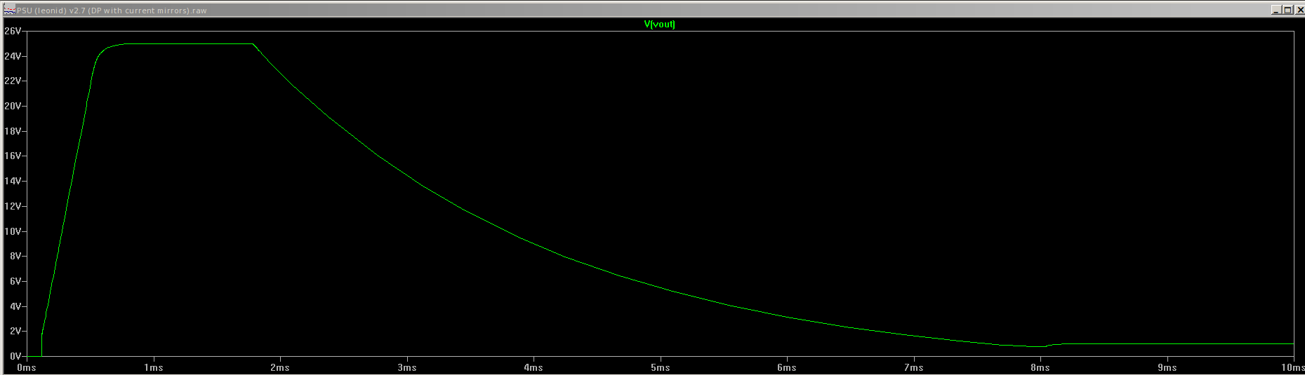
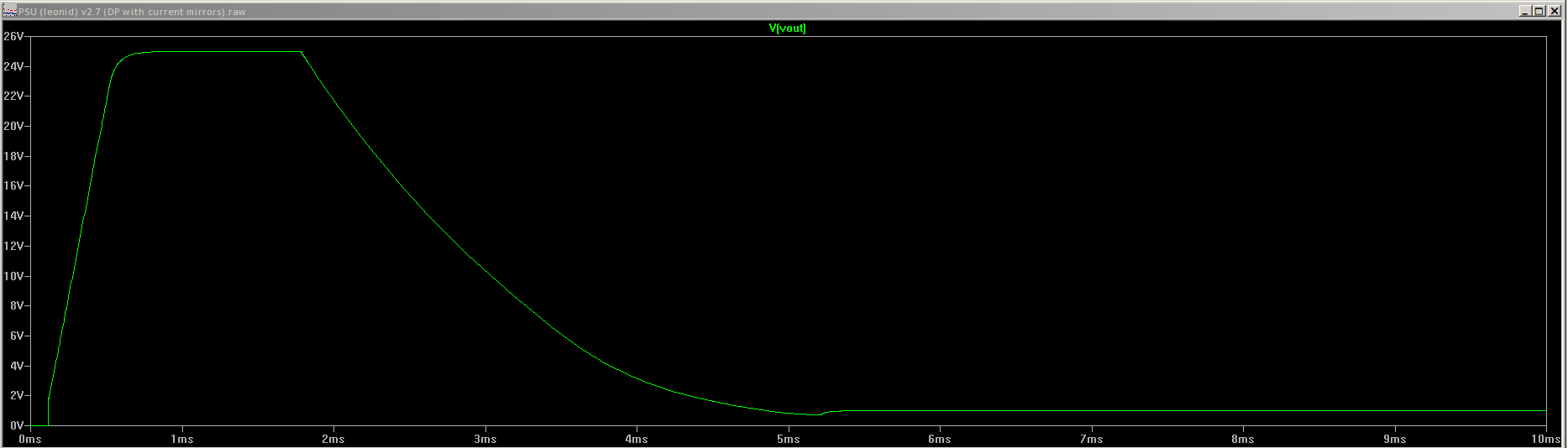
Here is how it looks like when Vout is controlled by sequence 5-7.5-10-7.5V sent using DAC. Notice difference in fall time:


New post-regulator include so-called down-programmer. I found this feature (check i.e. this and this Agilent documents) useful and decide to definitely test it and eventually add to the next PCB revision. Difference cannot be noticed with huge load (small impedance) but it’s clearly visible with smaller load or no load. Please find below two screenshots from simulations with down-programmer (DP) switched off and on:
Here is how it looks like when Vout is controlled by sequence 5-7.5-10-7.5V sent using DAC. Notice difference in fall time:
Attachments

- Home
- Design & Build
- Equipment & Tools
- DIY programmable dual channel bench PSU 0-50V/3A