...each FIR block only processes the left channel of an I2S stream, but this is good as it is easy to add more channels and still process both channels of a stereo I2S stream (most surround receivers I've seen use stereo pairs.)
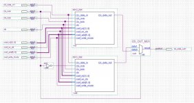
The attached screenshot shows how simple it can be to add more channels. You simply add a NOT gate to the LRCLK of the second block, then add a mux at the outputs to combine the data together. The result is a stereo filter.
To use this on surround data, or for crossovers, you just add more blocks (as long as they fit the FPGA.) I haven't done any accurate calcs on how big an FPGA is needed for decent length filter....
...but, a 2048 tap mono filter takes around 5% logic elements, and 81% memory bits of an Altera EP2C5T144 device. This is a cheap device and is used on the Pluto-3 board.....
http://www.knjn.com/ShopBoards_RS232.html
So, it could be used for say an 1200 tap stereo filter, and you would still have tons of logic left for a user interface (LCD), USB and all sorts.
Few actual logic elements are used for the FIR blocks even if more taps are added, so if the FPGA's memory blocks start to run low, I'm sure external RAM could be added instead of buying a more expensive FPGA.
(The coefficient inputs in the screenshot are connected to both channels for simulation, but it would be easy to load separate coefs for each block / channel.)
OzOnE.
Attachments
Hi all,
I'm posting my recent source code here as I received a request for some code. Although I've put a fair amount of work into it, it's not exactly revolutionary, and hopefully it will lead to faster development. Of course there will be many mistakes as I'm no expert, but if it was cleaned up a bit it might work quite well.
I'm now using a circular buffer for the data RAM. A circular buffer was really what I was after, but I only recently got my head around how it works. It's quite simple really (the diagrams on the Web could be a bit better.)
I'm now aiming to use external RAM which would free up the on-chip resources and should allow much longer filters (assuming they can be processed fast enough - or, you could use multiple processing blocks for each filter as the logic count of the block is low.)
OzOnE.
EDIT: Oh btw, the filter is set for 1024 taps to see how much RAM it would take, so the simulation doesn't work as it should because the input I2S stream is about 6 times faster than it would be in reality (for a 48KHz / 24bit stream.) There are probably errors in my I2S handling and all sorts, but it should in theory work with 1024 taps at 48KHz as long as the master clock is 60MHz or faster.
Attachments
Hi again,
Sorry, I think the last zip file had some errors in as it wouldn't work properly after reducing the taps. I've now attached a zip file which only has 32 taps so people can see more simply how it works. (or at least how it's supposed to work )
)
Please note that the coefficients will need to be loaded in reversed (so that the tail of the impulse is loaded first, and the peak is loaded last.)
Although I think this could be reversed quite easily for someone who knows what they're doing. 😉
OzOnE.
Sorry, I think the last zip file had some errors in as it wouldn't work properly after reducing the taps. I've now attached a zip file which only has 32 taps so people can see more simply how it works. (or at least how it's supposed to work
)Please note that the coefficients will need to be loaded in reversed (so that the tail of the impulse is loaded first, and the peak is loaded last.)
Although I think this could be reversed quite easily for someone who knows what they're doing. 😉
OzOnE.
Attachments
Hi Ozone-
Perhaps this link might be of some relevance to your project:
http://convolver.sourceforge.net/index.html
From my (obviously!) limited knowledge of DSP convolution execution, I would still say this project is very difficult. It is apparent that you have made significant progress towards a working solution, though!!
Kindest Regards,
Cliff
Hi, Cliff,
My knowledge of C++ programming is very limited. From a novice point of view, I would say that Verilog, or assembly language on PIC chips is easier to pick up than C++.
With C++, I can usually see how it works by reading the code, but writing my own code from scratch is difficult. I can't get to grips with all the ['s and ('s and ~'s and *'s!
btw, I had an idea for a fairly simple way of cascading the FPGA code modules so longer filters could be used (or higher sample rates).... When "latchin" happens in the controlblock, the first thing it does it to read the last word in the data RAM, then outputs this to "cascadeout" together with a "cascadelatchout". The signals will then go to another complete processing block, and the latchout from the second block will be used to latch the final result to the outputblock.
This will process the same filter length in half the time (with a few clocks added), but the coefficients will need to be split between each block. Or, it will process faster samplerates for the same length filter. So, if 50MHz is fast enough for 1024 taps at 48KHz, by cascading modules you could either do 2048 taps at 48KHz or 1024 taps at 96KHz.
The modules don't need many logic resources, so you could have long filters and mulitple channels. The only problem is how many RAM bits are available on the chip.....
The main issue I can see is that unless the master clock could be made much higher, it would be difficult to use one large external RAM for everything (due to the different addresses that need to be accessed). It would be a good idea to at least have separate data and coef RAMs though.
Does anyone have suggestions on how it would work with external RAM or SRAM?
OzOnE.
P.S. I've realized that the I2S modules would only work properly when the blck input was 48fs. It's not difficult to make it work at 64fs though.
Hello again Ozone-
The method you have described for cascading filter blocks in FPGA seems to be quite the common practice for high-speed filters utilizing very large counts of taps. There is a very good research paper called "FPGA Implementation of High Speed FIR Filters Using Add and Shift Method", done at the University of California, that might be of interest for you to read through. I don't have it available at the moment though, but it should pop right up through Google I think. I have also found that Mr. Ray Andraka has written a couple of great papers on getting the absolute most performance out of FPGA designs for DSP.
As far as using external RAM, from what I have read most Xilinx FPGAs are able to handle DDR RAM interfacing without too much work. I have found that there are often working examples of basic building blocks for these kind of things on opencores.org
I will keep an eye on this project and see where you take it. It seems that you're well able to get the DSP end of things done!😀
Hi Cliff,
I've read many of the white papers for this stuff on the "Interweb", but the problem for me is how to implement this kind of thing as I have zero knowledge of things like algebra and I've only really been using FPGA's for a couple of months.
I think I can get something working though, even if it's 2048 taps stereo to begin with. I just need to pull apart an old DVD player, solder my FPGA board before the DAC, and start messing about!
I've now added a cascade output to the control module.... The last tap is actually processed first atm which is good as it allows the last data word to be output to the next module. This is a fairly simple way of "bolting" modules together so the filters will be processed in parallel (ie. much faster.) Of course, this still requires more RAM bits, but allows much longer filters and higher samplerates (should be easier to make it work up to 192KHz).
When the coefficients are loaded in, they could be split between modules automatically using a simple address decoder....
eg. with two modules at 1024 taps each (2048 total), the first module will get coeffs 0 - 1023, and the second module will get coeffs 1024 - 2047.
As far as the RAM problem, I think it would need an awful lot of pins to add external RAM to make things process fast enough because I'm trying to do the processing using every tick of the master clock. This means that the data needs to be available on every tick, and for multiple blocks. I think if the external RAM had a wider output width (48 or more), then some sort of interleaving could be done. Probably using external RAM will allow a much faster master clock anyway, as the internal RAM seems to be a bottleneck atm.
All this is a bit of a headache as the complexity starts to increase exponentially when more taps are added etc. Simulation is also getting very difficult to organize.
It's all a learning experience though, and I'm still determined to get something running. The next setback is having to start work again "next year"! 😉
OzOnE.
P.S. A very Happy New Year to all! I'm gonna make it a good one damn it! 😎
Hi Ozone,
I took a quick look at your Verilog. It looks pretty solid overall.
However, I don't like this 😉 :
It's the state machine update for outputblock.v. This is going to synthesize into a funny blob on the state register clock input, since it has to accommodate two rising edge sources. It probably works fine, but messy clocking structures like these have a tendency to cause problems. The "safe" method is to choose one clock signal, with enables when needed.
You already have something like like this for loading the storage reg, but you'll have to rethink the module. I'm pretty sure there's a clean solution.
Your oneshot.v has a similar dual posedge statement. You can probably exchange that block for some combinational logic.
As for external memory, 12ns SRAM is readily available. SDRAM is also possible, with the minor trouble of interfacing and refreshing. Internal RAM is typically much faster than external.
HTH, and Happy New Year.
I took a quick look at your Verilog. It looks pretty solid overall.
However, I don't like this 😉 :
Code:
always @(posedge bclk or posedge latchen)It's the state machine update for outputblock.v. This is going to synthesize into a funny blob on the state register clock input, since it has to accommodate two rising edge sources. It probably works fine, but messy clocking structures like these have a tendency to cause problems. The "safe" method is to choose one clock signal, with enables when needed.
Code:
always @(posedge bclk)
if (latchen = 1'b1)
...
You already have something like like this for loading the storage reg, but you'll have to rethink the module. I'm pretty sure there's a clean solution.
Your oneshot.v has a similar dual posedge statement. You can probably exchange that block for some combinational logic.
As for external memory, 12ns SRAM is readily available. SDRAM is also possible, with the minor trouble of interfacing and refreshing. Internal RAM is typically much faster than external.
HTH, and Happy New Year.
Hi,
The reason I have "bclk" and "latchen" in the always statement of the output block is because the latchen input comes from the controlblock and is clocked by the master clock. The output block is only clocked by bclk, which is much slower than the master clock, so if the "latchen" part was added as an IF statement, I think the output block is likely to "miss" the latchen pulse.
The latchen input is really just a trigger input which latches the new input word then starts the process of outputting I2S data. It's not really an enable input as such, so I thought it would be better for it to work using posedge detection in the hope that it would synthesize combinational logic.
I seem to end up using the oneshot code all the time for making sure pulses only last for one clock period. It also delays the pulse for one clock cycle. I'm not sure of the methods for doing this quickly in code apart from adding extra bits to the state machines etc. I could probably use a delay command, but I don't know how much more than the basic code. Again, suggestions are always appreciated, as I'm still very much a newby to Verilog.
I think the oneshot code works by detecting it's own output pulse to reset the register. I have noticed it seems to add a fair bit of clock skew, and also limits the maximum clock speed. I've done away with it on the "latchen" output, and could probably do the same on the input. It usually just means adding an extra state to make sure the output pulse happens after the new data has arrived. It shouldn't be a problem to re-triggering because the processing takes a lot longer than one bclk period.
Also, I've now made the FIR block into a separate block and the input and output blocks are external to it. This allows the FIR blocks to be cascaded, but I'm still working out the bugs. I think I'll just use a short filter at first when I hook up my FPGA board to see if it works at all. The first step will be to pass the I2S data directly between the input and output blocks to make sure they work with the common bit widths etc. My board is only a 4000 gate Cyclone, but will be fine for initial testing.
SRAM would be the ideal way to go and I don't think any of the RAM needs to be dual ported as long as the controlblock code was changed so that new coeffs could be loaded etc.
I'm starting to remember why FPGA's are so good - it is so much easier to add features in the future and are generally more powerful than using a CPU (price wise). You could add things like DSD decoding and ASRC with a decent FPGA and mess around with dithering options. Ideally, this FIR filtering would be combined with something like peufeu's project.....
http://www.diyaudio.com/forums/showthread.php?s=&threadid=106497
OzOnE.
You have to be careful when writing in an HDL, because the underlying hardware resources (or synthesis tools, for that matter) can't always produce the behavior you desire. With your code, after synthesis and mapping, I see a state machine clocked on bclk, with latchen as an enable. So there won't be any activity on posedge latchen! (See attached)OzOnE_2k3 said:The reason I have "bclk" and "latchen" in the always statement of the output block is because the latchen input comes from the controlblock and is clocked by the master clock. The output block is only clocked by bclk, which is much slower than the master clock, so if the "latchen" part was added as an IF statement, I think the output block is likely to "miss" the latchen pulse.
The latchen input is really just a trigger input which latches the new input word then starts the process of outputting I2S data. It's not really an enable input as such, so I thought it would be better for it to work using posedge detection in the hope that it would synthesize combinational logic.
Oneshots are very useful. It may feel like a step backwards, but I try to think of little structures like oneshots in terms of registers and gates. Note that delay commands only work in simulation (to my knowledge).I seem to end up using the oneshot code all the time for making sure pulses only last for one clock period. It also delays the pulse for one clock cycle. I'm not sure of the methods for doing this quickly in code apart from adding extra bits to the state machines etc. I could probably use a delay command, but I don't know how much more than the basic code. Again, suggestions are always appreciated, as I'm still very much a newby to Verilog.
Broadly speaking, it's good to be familiar with the underlying hardware resources of the FPGA fabric. Try to write the HDL with an eye toward synthesis. Check the synthesized/mapped schematic as necessary to verify that you're getting the behavior you want.
FPGAs are fun, yes, when you finally get them working 😀. Cheers.
Attachments
Note that delay commands only work in simulation (to my knowledge).
You're right.
These are nice constructs for behavourial models but not for synthesis.
@OzOne
"The Design Warrior's Guide to FPGAs" from Clive Maxfield is a great way to start reading.
The crossing between one clock doamin into the other is , as you probably guessed clock-domain crossing, and is an all time favourite 😀 in literature and designs.The output block is only clocked by bclk, which is much slower than the master clock, so if the "latchen" part was added as an IF statement, I think the output block is likely to "miss" the latchen pulse.
One solution to pass data on form one clock domain to the others is to use a FIFO with a read and write port.
Depending on the implementation of the design the oneshot can be used as well
ST
Hello All-
I have read through this thread from the beginning, and now see there has been quite a lot of discussion about the Analog Devices SHARC DSP chips. There actually IS a "open-source" development method using a console-based compiler/linker through the "g21K" tools. These probably stop supporting the latest processors, though; more than likely not past the ADSP-2106x chips. There was also a company called "BeastRider" that made some quite affordable software tools for doing SHARC programming, but I have no idea where they have disappeared to, the beastrider.com site seems to be gone.
The FPGA companies seem to be keen to offer some pretty good basic programming tools for their chips, I wish this would carry over to the DSP processors as well. The VisualDSP++ suite is sure nice to work with, but the $3500 price tag will surely keep away anyone with a hobby-level budget!
FWIW - I have three large-format digital mixing consoles where I work, made by a British company called DiGiCo. These are based on the SHARC chips, each console has 30 ADSP-21062 chips and 6 more ADSP-21065L chips for special purpose processing. They will do up to 224 inputs and 224 outputs at 48k/24-bit resolution, or half of that at 96k/24-bit. So I know first hand that well-written, compact DSP code can do quite a lot of audio manipulation. They do sound VERY nice as well, with 40-bit floating point resolution on the internal mix bus....
Hi,
That's an impressive amount of audio those SHARC chips are throwing around! I've noticed those chips are increasingly popular and are showing up in many AV amps etc. (My Denon has two ADSP-21065L chips for example.)
It would be great to start programming on a SHARC, but as you say, the development tools can be pricey. Also, if I were to use open-source compilers I think it would take more learning time to get things running as these tools often lack a graphical IDE.
The thing about working with FPGAs is that what I'm trying to do is quite a straightforward process (once I got my head around it) so I'm dedicating the chip resources to the specialist task of full-range FIR filtering. This should hopefully mean a cheaper and quicker route to a solution.
I don't doubt the power and flexability of the SHARC chips, but I'm guessing the learning curve would be quite a bit steeper. If I could find an affordable SHARC dev board that would be able to process a fair few channels then I might give it a go in the future.
As far as the FPGA project - I now have the board hooked up to my Freeview (DVB-T) box! I cut the track between the main processor's audio data output pin and the DAC, then put the FPGA board between the two point. The LRCLK and BLCK lines are then routed to the FPGA as well.
The first step was to test the input and output block code. For some reason which I still can't figure out, the audio was actually left-justified as opposed to I2S justified. The datasheet shows that this chip (CS4334) should be I2S? It took me around three days to get it working properly without the serious clipping I was getting.
What I did in the end (and what I should have done from the start ) was to hook up the o'scope and compare the input to the output. I then noticed that the audio bits were shifted right one BCLK instead of being clocked out directly after the falling edge of LRCLK.
So anyway, I seem to be able to pass the audio through the input and output blocks without serious problems now. The audio quality isn't 100%, but that's mainly because the DAC needs 5V inputs and the FPGA is not 5V tolerant. I'm only using resistors to protect the FPGA inputs atm which isn't ideal.
I've now also got the FIR block to work, but the audio quality is terrible. This must be mainly due to the "rounding" at the output of the MAC block. I'm not really doing a proper rounding at all but simply dividing the result down to fit the 24bit output. But, it does show that the FIR block seems to be working. (I'm testing with a single "1" as the first tap coeff, so it should pass input to output untouched.)
I had a lot of problems getting to this point, and only realized yesterday why I wasn't getting audio at all with a 512 tap filter length - this was due to me forgetting I only have a 25MHz master clock on the FPGA board! (This can only barely process a 128 tap filter.) I've now changed the simulation waveforms to reflect the true master clock rate and audio sample rate.
Surprisingly, my Digibox does actually output 24bit data to the DAC. I always thought standard audio on Freeview / Sat / Cable was 16bit at 48KHz? So, this digibox is probably upscaling the audio to 24bits.
Just to note: the relatively low master clock rate of this board doesn't necessarily limit the filter length as we should still be able to cascade the FIR blocks in parallel to process much longer filters.
Another thing I've noticed is that if I pass the data between the input and output blocks, the audio sounds OK (ish), but it looks like the output block is not outputting the MSB (sign bit)? This would mean the output of the DAC will always stay positive (can't be good.)....
This is because there is still a delay of one BCLK before the data is actually output. To fix this, I could just add a simple counter to count the number of BLCKs per sample then use this as a timing reference.
So, it seems to be working in theory but I've got quite a bit of work to do before I can be confident that the initial idea is working as it should.
At this moment, I'm taking the lower 24 bits of the filter result and using that as the output directly. This will test to see if the filter is contributing to the audible issues I'm hearing. (The filter result will not saturate above 24 bits because I'm only using one "1" as a coeff for testing.)
OzOnE.
P.S. If anyone wants, I can attach the most recent project here. I've now got a fairly good way of handling the clock domain crossing by using a simple handshaking block.
That's an impressive amount of audio those SHARC chips are throwing around! I've noticed those chips are increasingly popular and are showing up in many AV amps etc. (My Denon has two ADSP-21065L chips for example.)
It would be great to start programming on a SHARC, but as you say, the development tools can be pricey. Also, if I were to use open-source compilers I think it would take more learning time to get things running as these tools often lack a graphical IDE.
The thing about working with FPGAs is that what I'm trying to do is quite a straightforward process (once I got my head around it) so I'm dedicating the chip resources to the specialist task of full-range FIR filtering. This should hopefully mean a cheaper and quicker route to a solution.
I don't doubt the power and flexability of the SHARC chips, but I'm guessing the learning curve would be quite a bit steeper. If I could find an affordable SHARC dev board that would be able to process a fair few channels then I might give it a go in the future.
As far as the FPGA project - I now have the board hooked up to my Freeview (DVB-T) box! I cut the track between the main processor's audio data output pin and the DAC, then put the FPGA board between the two point. The LRCLK and BLCK lines are then routed to the FPGA as well.
The first step was to test the input and output block code. For some reason which I still can't figure out, the audio was actually left-justified as opposed to I2S justified. The datasheet shows that this chip (CS4334) should be I2S? It took me around three days to get it working properly without the serious clipping I was getting.
What I did in the end (and what I should have done from the start
) was to hook up the o'scope and compare the input to the output. I then noticed that the audio bits were shifted right one BCLK instead of being clocked out directly after the falling edge of LRCLK.So anyway, I seem to be able to pass the audio through the input and output blocks without serious problems now. The audio quality isn't 100%, but that's mainly because the DAC needs 5V inputs and the FPGA is not 5V tolerant. I'm only using resistors to protect the FPGA inputs atm which isn't ideal.
I've now also got the FIR block to work, but the audio quality is terrible. This must be mainly due to the "rounding" at the output of the MAC block. I'm not really doing a proper rounding at all but simply dividing the result down to fit the 24bit output. But, it does show that the FIR block seems to be working. (I'm testing with a single "1" as the first tap coeff, so it should pass input to output untouched.)
I had a lot of problems getting to this point, and only realized yesterday why I wasn't getting audio at all with a 512 tap filter length - this was due to me forgetting I only have a 25MHz master clock on the FPGA board! (This can only barely process a 128 tap filter.) I've now changed the simulation waveforms to reflect the true master clock rate and audio sample rate.
Surprisingly, my Digibox does actually output 24bit data to the DAC. I always thought standard audio on Freeview / Sat / Cable was 16bit at 48KHz? So, this digibox is probably upscaling the audio to 24bits.
Just to note: the relatively low master clock rate of this board doesn't necessarily limit the filter length as we should still be able to cascade the FIR blocks in parallel to process much longer filters.
Another thing I've noticed is that if I pass the data between the input and output blocks, the audio sounds OK (ish), but it looks like the output block is not outputting the MSB (sign bit)? This would mean the output of the DAC will always stay positive (can't be good.)....
This is because there is still a delay of one BCLK before the data is actually output. To fix this, I could just add a simple counter to count the number of BLCKs per sample then use this as a timing reference.
So, it seems to be working in theory but I've got quite a bit of work to do before I can be confident that the initial idea is working as it should.
At this moment, I'm taking the lower 24 bits of the filter result and using that as the output directly. This will test to see if the filter is contributing to the audible issues I'm hearing. (The filter result will not saturate above 24 bits because I'm only using one "1" as a coeff for testing.)
OzOnE.
P.S. If anyone wants, I can attach the most recent project here. I've now got a fairly good way of handling the clock domain crossing by using a simple handshaking block.
As for channels, the usual dev board comes with an 8 channel DAC.
If you don't have enough MIPS, you can always move up to TigerSHARC
If you don't have enough MIPS, you can always move up to TigerSHARC
Originally posted by OzOnE_2k3
At this moment, I'm taking the lower 24 bits of the filter result and using that as the output directly. This will test to see if the filter is contributing to the audible issues I'm hearing. (The filter result will not saturate above 24 bits because I'm only using one "1" as a coeff for testing.)
Are you sure you don't mean the upper 24 bits? Because that's what you should be using - the 24 most-significant bits.
Simply taking these bits (i.e., not dithering) as the output is fine at this stage - it works perfectly well, you just get a teeny tiny amount of distortion. Adding dither really is icing on the cake, so leave it until much later.
I really do wonder, given that 24 bit audio DACs are not linear to 24 bits, what does it matter what's in the LSB? Truncation would probably make no difference whatsoever.
One of the most linear DACs is the AD1955, and you can see that it's only linear to -125 dB, rather than the theoretical -140 dB for 24 bits (TPC.12). The rest of it looks like they scramble so it doesn't have signal-correlated distortion. Compare to the AD1853 which has weird crap going on under the king at -115 dB.
BTW, anyone know why TI doesn't put linearity graphs in their DAC datasheets? I always found that suspicious.
They probably figure it doesn't matter. Just like how audio DACs don't specify INL/DNL. TI's 20-bit industrial DAC has a settling time of 2ms, so the audio DACs must be doing something sketchy under the hood. They seem to sound OK, though. <shrugs>
If I'm using the DSP for oversampling filter, is there any issue in oversampling by a non-integer ratio? I don't want to have to use two clocks to handle separately the 44.1 and 96 kHz sample rates, since high quality clocks are very expensive. So I'm thinking of oversampling in both cases to 384 kHz (it's for AD1955 DAC).
Hi,
@Wingfeather - I forgot that you mentioned using the upper bits before. I think I have bigger issues though....
If I create my own simple "filter" by entering coeffs manually in a text file I can actually get some sort of filtering happening now without tons of distortion / clipping. When I say a simple filter, I mean very simple like using taps of 1 2 3 4 5 repeating every 32 taps or something like that - I'm not using proper filter coeffs yet due to the problems below....
The main issue is that I have to use integers as the code currently only has an integer MAC block. The MAC is set for signed data and it does work as expected with negative numbers, but I've now entered the minefield of Q15 / Q24 formats etc....
I only recently found out about the "Q" format and why it is used in DSP. As far as I understand so far, the basic process is to use fractions instead of integers to represent the samples (and taps). So, in many audio formats, they use something like 0.32624524 for a sample (or anything below "1"). When two of these numbers are multiplied, the result is always less than "1".
So, does that mean that I would be able to convert the audio and filter taps to signed integers and still get fairly good audio quality, or is it best to design everything to use "Q" format samples / taps to begin with?
Which format is the "standard" used on most DACs? Is it just signed integers (two's complement)? Where, with 16 bits, the minimum and maximum sample values would be....
-32767 and +32768 ?
Basically, is there a difference between the "standard" format for 16bit / 24bit audio sent to DACs, and the "standard" format used to store 16bit / 24bit audio in a file?
Please help, I'm very confused now. I thought I was close to a partially working design, but I can see there are still many hurdles. I still believe FPGAs are a good solution for price / performance ratio and flexability though.
OzOnE.
@Wingfeather - I forgot that you mentioned using the upper bits before. I think I have bigger issues though....
If I create my own simple "filter" by entering coeffs manually in a text file I can actually get some sort of filtering happening now without tons of distortion / clipping. When I say a simple filter, I mean very simple like using taps of 1 2 3 4 5 repeating every 32 taps or something like that - I'm not using proper filter coeffs yet due to the problems below....
The main issue is that I have to use integers as the code currently only has an integer MAC block. The MAC is set for signed data and it does work as expected with negative numbers, but I've now entered the minefield of Q15 / Q24 formats etc....
I only recently found out about the "Q" format and why it is used in DSP. As far as I understand so far, the basic process is to use fractions instead of integers to represent the samples (and taps). So, in many audio formats, they use something like 0.32624524 for a sample (or anything below "1"). When two of these numbers are multiplied, the result is always less than "1".
So, does that mean that I would be able to convert the audio and filter taps to signed integers and still get fairly good audio quality, or is it best to design everything to use "Q" format samples / taps to begin with?
Which format is the "standard" used on most DACs? Is it just signed integers (two's complement)? Where, with 16 bits, the minimum and maximum sample values would be....
-32767 and +32768 ?
Basically, is there a difference between the "standard" format for 16bit / 24bit audio sent to DACs, and the "standard" format used to store 16bit / 24bit audio in a file?
Please help, I'm very confused now.
I thought I was close to a partially working design, but I can see there are still many hurdles. I still believe FPGAs are a good solution for price / performance ratio and flexability though.OzOnE.
Hi Ozone,
The idea of fractional or integer mathematics is largely irrelevant - it's all about how you think about the numbers in question. For example:
In fractional, 0.5 * 0.5 = 0.25. Done as a signed 32x32->64 multiply:
0100 0000 0000 0000 0000 0000 0000 0000
*
0100 0000 0000 0000 0000 0000 0000 0000
=
0010 0000 0000 0000 0000 0000 0000 0000 0000 0000 0000 0000 0000 0000 0000 0000
If you think about alignments of things, you're basically keeping the MSB as aligned with the value of -1, regardless of word length.
In integer format, 2^31 * 2^31 = 2^62. Here, you're aligning the LSB with an integer value of 1, regardless of word length. Note that the binary representation of this calculation is the same as for the fractional one. The operands and the result are the same, it's just a different way of thinking about it.
I hope that makes it clearer.
People generally prefer to think of numbers in fractional format because the values are constrained between plus and minus one, and it simplifies things. The number of bits only changes the amount of precision you have. With integer, a change in word-length actually changes the size of the values and things get a bit weird.
But again, it's all the same, really. For 32-bit filter coefficients, I tend to use a 2.30 format, since filter coefficients often require a range between plus- and minus-two. There's no difference in the multiplier itself, the result just needs to be interpreted differently.
In all cases, though, the result of a calculation should be taken as the top X bits of what comes out of it.
As for DACs and things, they use two's-complement format as here. The idea of a decimal point - or even absolute value - is useless because all the audio is doing is moving between plus- and minus-full-scale. You can think of it however you like. 🙂
- Status
- Not open for further replies.
- Home
- Source & Line
- Digital Source
- DIY DSP for Digital Room Correction