I see this other schematic with reversed drain/source IRF610 position
Wich one is the correct?
An externally hosted image should be here but it was not working when we last tested it.
Wich one is the correct?
sources are down ( to negative ) and drains are up ( to positive ) ;
I never look at symbols in schematic , mostly because I just can't remember what's source and what's drain on them ......
so - those details - mistakenly reversed symbols , reversed caps and zeners - I usually can't spot them
I never look at symbols in schematic , mostly because I just can't remember what's source and what's drain on them ......
so - those details - mistakenly reversed symbols , reversed caps and zeners - I usually can't spot them
Please check the datasheet of the dac.
measure dc at the source of t1a/b and/or the output pins of the dac. should be the same.
How is it all wired up?: cdplayer/i2s signal -> reciever/dac -> i/v?
regards
Output pins DAC & source of t1a/b both channels -0.740VDC, so it's the same in DAC like in the I/V.
Is wired: PC usb // HiFace usb receiver s/pdif output // CS8414 receiver PCM1704 DAC SE.
Thks for help.
sources are down ( to negative ) and drains are up ( to positive ) ;
I never look at symbols in schematic , mostly because I just can't remember what's source and what's drain on them ......
so - those details - mistakenly reversed symbols , reversed caps and zeners - I usually can't spot them
Thks ZM, so my schematic is OK, right?
Thks ZM, so my schematic is OK, right?
yes - schematic from http://www.diyaudio.com/forums/pass-labs/181449-diy-d1-i-v-stage-2.html#post2534689 is correct - sources pointing down
PCM1704 - if connected by datasheet - have 0 offset at output
connect D1 to it , then you must set - with P1 - that you still have 0V at PCM output/D1 input
rest is irrelevant
PCM1704 Left channel 0.004V Right channel 0.006V so 0 offset but now the I/V input is in both channels -29.5VDC & the trimmer can modifie the value so is fixed -29VDC both inputs channels😕
PCM1704 Left channel 0.004V Right channel 0.006V so 0 offset but now the I/V input is in both channels -29.5VDC & the trimmer can modifie the value so is fixed -29VDC both inputs channels😕
give us complete schematic of PCM stage you are using
we are looping this way - you obviously didn't understood what's written
I don't have the schematic it's an Elektor Audo DAC 2000 without I/V Audio DAC 2000 (3) - ELEKTOR.com | Electronics: Microcontrollers Embedded Audio Digital Analogue Test Measurement
PCM1704 measurements are done disconnected from I/V, I/V mesurements are done without PCM1704 connected.
PCM1704 measurements are done disconnected from I/V, I/V mesurements are done without PCM1704 connected.
before connecting D1 to PCM - you need to set P1 to have approx. 0V at I/V input , measuring against gnd
then you connect D1 to PCM , power up everything and do fine setting after some time ( when everything is in temp. equilibrium .
simple as that .
if something is not working - something is dead .
either PCM or D1 .
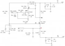
edit :
schematic with approx. voltages attached ; what is important is just red 0V value ;
all other voltages approximately , and valid only for troubleshooting purpose
then you connect D1 to PCM , power up everything and do fine setting after some time ( when everything is in temp. equilibrium .
simple as that .
if something is not working - something is dead .
either PCM or D1 .
edit :
schematic with approx. voltages attached ; what is important is just red 0V value ;
all other voltages approximately , and valid only for troubleshooting purpose
Attachments
Last edited:
Thanks, I/V 0Vdc at input, now I have to check DAC because is moded with a clock at the receiver CS8414 so must check all.
before connecting D1 to PCM - you need to set P1 to have approx. 0V at I/V input , measuring against gnd
then you connect D1 to PCM , power up everything and do fine setting after some time ( when everything is in temp. equilibrium .
simple as that .
if something is not working - something is dead .
either PCM or D1 .
edit :
schematic with approx. voltages attached ; what is important is just red 0V value ;
all other voltages approximately , and valid only for troubleshooting purpose
While adjust DAC I measured I/V:
Left channel
R6 // Drain T1 // C3 14.20V
R5 // Gate T1 // C2 // P1 3.45V
C5 // Source T2 // R4 10.77V
R2 // Source T1 0 V
Right channel
R6 // Drain T1 // C3 14.17V
R5 // Gate T1 // C2 // P1 3.45V
C5 // Source T2 // R4 10.74V
R2 // Source T1 0 V
Are the measurements right?
obviously yes ;
I told you - all voltages are just approx , counting roughly that Ugs of mosfet is 4V
that 0V point is what is important/needs setting
I told you - all voltages are just approx , counting roughly that Ugs of mosfet is 4V
that 0V point is what is important/needs setting
After 9 days of extensive listening sessions I can conclude that sounds a lot better CS8414+DF1704+PCM1704+D1 I/V NP than BII+Legato in single end & balanced mode vs single end mode PCM1704+NP D1 I/V, details:
CS8414+DF1704+PCM1704 with Erno Borbely series regulators (one +5V (CS8414+DF1704 & two +-5V for PCM1704, NP D1 I/V LM317+LM337 for +-30V
BII+Legato with Salas regs V1.2R for BII, Salas reg V1.0 remote sense for Legato & set of 3 Trident regs for BII
I use Sony Vaio laptop like source, both share USB 2.0 HiFace with Salas 1.0 remote sense reg
N.B. Erno Borbely adviced me that PCM1704 sounds better than BII, next step I will change Legato I/V for Classic Pass Labs D1 I/V with an ESS Dac designed by Owen (opc)
- Status
- Not open for further replies.
- Home
- Amplifiers
- Pass Labs
- DIY D1 I/V STAGE