Hysteresis amps are a bit more amenable to intuitive analysis and therefore may be a more practical starting point for beginners. I began that way 🙂
One important thing: Get the positive (=hysteresis) feedback from the power stage as well, not from the comparator output. Otherwise you'll find the switching frequency changing with power supply voltage.
A good hysteresis value is 1/1000.
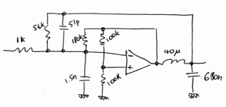
Attached is a drawing which I put up earlier somewhere (it could have been this thread), showing a hysteresis amp with mixed feedback. The "comparator" symbol includes the switching stage.
One important thing: Get the positive (=hysteresis) feedback from the power stage as well, not from the comparator output. Otherwise you'll find the switching frequency changing with power supply voltage.
A good hysteresis value is 1/1000.
Attached is a drawing which I put up earlier somewhere (it could have been this thread), showing a hysteresis amp with mixed feedback. The "comparator" symbol includes the switching stage.
Attachments
Hi Bruno,
...great to get your support!
To pick also the positive feedback from the power stage was exactly, what I tried first in an older set up, with a discrete differential and some crosswise full symmetric feedback of the full bridge . But simulation surprised me with some difficulties in proper oscillation, sometimes. It was caused by the neg feedback, which acted so earlier, due to improper delays of the two halfbridges.
Unfortunately the halfbridge which should give the pos feedback acted later than the other one.....
By picking the positive feedback from the comparator oscillation became perfectly reliable, because this shifted the small time delay between positive and negative feedback to the desired direction (comparison level definitely has jumped before the neg feedback can change anything..).
Anyway, I will try your proposal here again. As in this circuit positive and negative feedback are derived by the same halfbridge, I think it should work fine.
Frequency modulation with changing rail voltage:
Is frequency modulation a major concern?
I took care about the neg feedback to be picked from the power stage, because the gain of the power stage is directly proportional to the rail volatge.
But which drawbacks will I face due to some variation in the switching frequency?
Feedback level about 1/1000:
So according your experience my ramping level of several hundrets of millivolts at the input stage is high above the optimum?
You would prefer ramping levels around +/50mV, correct?
Due to possible issues with saturation in the comparator input stage?
Bye
Markus
Hello,
I think the problem with frequency modulation lies simply in limiting it to a desired value, so that it doesn't start at say 100khz and wind up at 2Mhz. It's an extrem example but gives you the idea.
To avoid that you have to have the hysteresis set points ride the reference signal, and the control signal as well. That stabalizes the switching frequency a fair amount. It's not easy though, after many many failed attempts, I'm a little afraid of the hysteresis modulator these days. Phase modulation is easier for me to grasp the concept of, there's alot more material out there to be found on phase shift oscillators/circuit examples etc than there are for hysteresis modulators.
I would like to learn more about them as well. Bruno actually emailed me a full circuit schematic of his SODA amplifier over a year ago, and I learnt alot from it, but I couldn't figure out the hysteresis aspect of it, never tried duplicating it either, or match it to what I thought I wanted to achieve (mueta). After having read the mueta patent, it's a little more complicated than I'd first assumed, to say the least.
I sure would like to try getting one going though (hys. modulator, not mueta), call it a grudge at this point.
Regards,
Chris
but I couldn't figure out the hysteresis aspect of it,
It is basically the same circuit one uses when building a rectangular oscillator with an op-amp, improved by an overall feedback loop.
Regards
Charles
Hang on... are you saying you were using one half bridge for the hysteresis and the other one for the feedback? The two half bridges will never operate identically, so you need to use both for the negative feedback (even if you decide to use comparator feedback for hyst.).
Attached is how to make a simple full-bridge self-oscillating amp. This circuit is used in this product (and others in that range).
http://www.bwspeakers.com/index.cfm/fuseaction/products.models/label/Model ASW CDM
The disadvantage of allowing the switching frequency to change with power supply is not enormous, unless you intend the circuit to operate over a wide supply range. It's just nice that you can have one modulator setting that you don't have to change when making new amps based on the same circuit.
The frequency swing with signal of hysteresis amps is already quite large. Increasing hysteresis will make this situation worse (capacitor charging can no longer be simplified as a linear ramp). If the gain of your amp is small, larger hystereses are not such a big problem, but if you want to have a gain of 30, well...
Attachments

....as expected, in my current schematic there are no big issues if I pick
the pos feedback from the power stage. For this, I disconnected R9 from "HB" and wired it to the center tap of the left halfbridge. I adjusted the value more or less according the increased voltage swing to 39k, may be 33k would match best....
I worked fine, but the distorsions doubled....???
May be the starting conditions of the outputfilter does not match anymore to the new slightly higher switching frequency???
Harmonics analysis with simulation is a mess as soon as you reach distorsion levels below 1%.... (just IMHO)...
Bye
Markus
Yepp, I adjusted the frequency back to it's former value (more or less).
Now my former adjustment of the starting conditions for the capacitors and inductors are matching well again.
THD is even slightly better, than in the first posting. Now: 0.02%
Dear Bruno,
...saw your last posting right now.
Yes, in one of my simulations, I picked pos feedback and neg feedback from different halfbridges..., ... not so good 🙄 ... I agree...
In my current simulation I am picking pos and neg feedback from the same halfbridge. The second halfbridge is running simply inverted with additional control.
My next step would be to use a differential amp for an additional outer feedback/gain-system. The feedback would be picked from behind the filter, from both bridge tails. I will post the schematic and the results, after finishing.
But I think the THD is already quite good and simulation results seem to be dominated from not perfectly matching start conditions of the capacitors and inductors. In real life the additonal outer loop may be more important.... as the real life full bridge will be not as nice as my simplified model...
By the way: Do you have a special trick for perfect start conditions?
I cannot let run the simulation for thousands of signal periods just in order to get correct steady state values....
Bye
Markus
...good schematic hint in your attached small gif-image....
Thanks!
Will help me with my older approach...
Thanks!
Will help me with my older approach...
You mean the second half bridge is running off the same comparator but the feedback loop doesn't see it? That is just as bad as the previous case.ChocoHolic said:In my current simulation I am picking pos and neg feedback from the same halfbridge. The second halfbridge is running simply inverted with additional control.
Try wobbling the power supply to see what I mean. PSRR=0
ChocoHolic said:By the way: Do you have a special trick for perfect start conditions?
In the rare instances that I perform time-domain simulations, I do so with an "idealised" power stage. I don't ever simulate complete amps.
I'm a bit bemused by the local hobby in this thread of trying to optimise a class D amp on a spice simulation.🙄
Hi Bruno!
Glad to hear your opinion on optimizing everything with simulation....
I am 200% with you in this regard!
PSSR=0?
Doesn't the second halfbridge bring a system inherent high PSSR?
As you switch the rail modulation in positive AND negative direction to the load, the low frequency modulation in the load current should be very low... I thought... ???!!!
....hm, I think you might be right.... uhps!
If the feedback is from one end only, then the rail modulation will be given non compensated to the input......
Anyway, I am already simulating your cross symetric proposal.
Apart from some convergence issues (as usual) it was working fine from the very beginnig. I split the ramping cap and put the center tap to ground in order to overcome this....
...before this the differential showed heavy common mode jumping, because the power stages do not always switch perfectly at the same time....
Attached file shows the full symmetric arrangement.
Bye
Markus
Glad to hear your opinion on optimizing everything with simulation....
I am 200%
with you in this regard!PSSR=0?
Doesn't the second halfbridge bring a system inherent high PSSR?
As you switch the rail modulation in positive AND negative direction to the load, the low frequency modulation in the load current should be very low... I thought... ???!!!
....hm, I think you might be right.... uhps!
If the feedback is from one end only, then the rail modulation will be given non compensated to the input......
Anyway, I am already simulating your cross symetric proposal.
Apart from some convergence issues (as usual) it was working fine from the very beginnig. I split the ramping cap and put the center tap to ground in order to overcome this....
...before this the differential showed heavy common mode jumping, because the power stages do not always switch perfectly at the same time....
Attached file shows the full symmetric arrangement.
Bye
Markus
Attachments
The overall design is as simple as I never thought, that it could be possible. Just two transistors, some resistors, one cap and a full bridge. COOL!!!
The simplified full bridge should reflect quite good the behavoiur of my plans with the LM5104 driven bridge. In some months I can give a comment about that driver chips and how their adaptive dead time is working. For shut down, I am planning to trigger a latch which pulls down the supply voltage of the LM5104 to a value short below under the treshold of the UVLO. Under this condition the gates of the Mosfets will pulled down.... Let's see how it will work.
Bye
Markus
ironless torroid choke
...with respect to the idea of an ironless choke...
I calculated an simple plastic torroid.
Dimension of the plastic core:
Outer diameter: 50mm
Inner diameter: 30mm
Height: 20mm
The basic formula
L=µ0 x µr x A x N^2 / le
leads to about 100 turns if you want 40µH....
Well sounds possible, but not very practical....
A ferrite solution is smaller and less lossy.
Yup... Went down the same road not so long ago. I was looking for an air coil that wouldn't produce a significant external field. Arrived at the same conclusion: too many turns. It looked so promising
Hi,
As for myself, it's a learning experience, and I would never have learnt anything regarding charge ratio/body diode recovery etc playing around with ideal switch devices in spice. Let alone even on how to drive one properly.
That said, now that I'd like to see how well it can work without any associated hassles brought on by the mosfets and their poor modeling, aaaand that I finally have a very straightforward example of how to use an ideal switch as a mosfet, thanks to Markus, I will be giving that a try as well.
Markus, looks like it's comming along great! I will have to try this.
Regards,
Chris
In the rare instances that I perform time-domain simulations, I do so with an "idealised" power stage. I don't ever simulate complete amps.
As for myself, it's a learning experience, and I would never have learnt anything regarding charge ratio/body diode recovery etc playing around with ideal switch devices in spice. Let alone even on how to drive one properly.
That said, now that I'd like to see how well it can work without any associated hassles brought on by the mosfets and their poor modeling, aaaand that I finally have a very straightforward example of how to use an ideal switch as a mosfet, thanks to Markus, I will be giving that a try as well.
Markus, looks like it's comming along great! I will have to try this.
Regards,
Chris
Hi Chris!
If you use the sbreak devices:
Please note that their default values are often not suitable.
Ron = 1 Ohm
Roff = 1 E6 Ohms
But you can easily change this in the "breakout.lib".
breakout.lib can be opened with most text editors
like Wordpad etc...
In this text file you must look for the model of the sbreak and
there you can change the default value. Depending on the PSPICE based program and version you can sometimes change the properties more comfortable, but the text editor should work always..... 😀
The sbreak changes its resistance from Roff towards Ron by a nonlinear function of the voltage, which is applied to the control pins.
0V ==> Roff (negative voltages ==> also Roff)
1V ==> Ron (higher control volatge ==> also Ron)
Please note also that convergence of the simulation algorithm is getting more difficult as higher the ratio Roff/Ron is chosen.
For my simulation, I changed Ron to 0.032 Ohms which corresponds to the IRFB52N15D...
I also appreciate simulation to learn about some basics.
But for detailed optimization it is not well suited.
Good Luck
Markus
Hi Markus!
Many thanks for those tips that should make life alot easier. What threw me before was not having thought of adding the Vth to the control pin, and instead tried to implement it by editing the on/off thresholds of the device which didn't seem to work well at all. Seems so much more straightfoward to just add a DC source like you've done.
Thanks again.
Chris
Hi Bruno,
From the above quote it might be understood that you mostly simulate in frequency domain. While I am familiar with averaged switching stage models from Dr. Ray Ridley for classic PWM stages, I am interested what type of model do you use for self oscillating power stages. In rare occasions when i simulated in frequency domain, I simply used amplitude limited E source and that seemed to do the trick. But I am not absolutely sure if that is the proper way.
Best regards,
Jaka Racman
In the rare instances that I perform time-domain simulations, I do so with an "idealised" power stage. I don't ever simulate complete amps.
From the above quote it might be understood that you mostly simulate in frequency domain. While I am familiar with averaged switching stage models from Dr. Ray Ridley for classic PWM stages, I am interested what type of model do you use for self oscillating power stages. In rare occasions when i simulated in frequency domain, I simply used amplitude limited E source and that seemed to do the trick. But I am not absolutely sure if that is the proper way.
Best regards,
Jaka Racman
Thanks Charles,
I suppose it works for you both in time and frequency domain?
Best regards,
Jaka Racman
I suppose it works for you both in time and frequency domain?
Best regards,
Jaka Racman
I suppose it works for you both in time and frequency domain?
To me it looks actually quite strange, but yes it does. The "etable" is basically a voltage controlled voltage source that allows some parameters to be set. I set it in a way that it acts like a stage with very high gain and a min and max output voltage of the desired p-p voltage.
The strange thing is that it has veeeeeeery high gain for the AC simulations in that case; and that's where I have problems understanding it. Simulated circuits, that should theoretically be unstable, behave nicely 😕 But maybe I just make a thinking error.....
Regards
Charles
- Status
- Not open for further replies.
- Home
- Amplifiers
- Class D
- Distorsions in class D