My smt experience:
I have never been successful using even very fine tipped tweezers to hold the part while soldering (parts are too thin so tweezer tips tend to contact the pcb before the part is resting on the pads, also you need to be very steady and compromising between movement and pressure).
Instead what works well for me is to place the part on the pads using fine tweezers and then lightly hold the part in place with a fine wood stick (toot-pick diameter and cut to form a feathered wedge on the tip, this allows one to make gradual contact without moving the part).
This works for me in conjunction with:
While lightly holding the part in place with the wood stick touch one end with the soldering iron (pre-applied tiny dot of 63/37 solder). Then solder the other side with a small solder feed, repeat for the first side.
I don't pre-apply solder on one pad (tilts the part and creates movement while soldering), exceptions are very fine pitch where I will apply then wick the solder prior to placing the part.
Liberal use of flux prior to placing the part (keeps the part in place while you let go of the tweezers, sometimes a little nudging is needed after letting go), this is really my key, does mean that an alcohol bath and brush necessary later.
Of course you need some fairly high magnification visors (age dependent).
Thanks
-Antonio
Yes, it requires some dexterity & practice to place the part. For passives, it is easy, pick/move the part as it sits on the PCB. Put the part close to the pad area. The tweezers will bottom out against the PCB, insta cal, it really is quite simple, once you get the hang of it!! Lots of light req. I am fortunate in this regard, I am myopic Rick
Last edited:
SUMMING AMP applications questions
I maybe showing my amateurism here but has this application been looked into either the SWfetJE990 or the SWOPA when the positive input is grounded and the negative input is used as a summing amp applications with very little gain? I have a schematic of a PRINCETON APPLIED RESEARCH 113 preamp in which the input is jfet and there are two inputs and two outputs, balanced in and balanced out, obviously for test purposes, but the gain can be selected from a gain of 1, 10 or 100. Don't think I can post the EEG schematic. Thanks, Ray😀
I maybe showing my amateurism here but has this application been looked into either the SWfetJE990 or the SWOPA when the positive input is grounded and the negative input is used as a summing amp applications with very little gain? I have a schematic of a PRINCETON APPLIED RESEARCH 113 preamp in which the input is jfet and there are two inputs and two outputs, balanced in and balanced out, obviously for test purposes, but the gain can be selected from a gain of 1, 10 or 100. Don't think I can post the EEG schematic. Thanks, Ray😀
now I will have to go and look up ME...............@AndrewT, I am surprised that you had to look up HASL, but you did state that you are an ME by profession.............
I suspect your are wrong.
Have you checked my profile?
AndrewT, I thought that I read in one of your replies, I will never be able to find it, that you stated that you were a Mechanical Engineer. I could be wrong, did not want to insult you in anyway, us EE types, used to make fun with ME's, just a bit of technical rivalry amongst the design team. Same as as with the SW/FW folks, its a HW problem, no its a SW problem, all in good fun. Engineering can be stressful, gotta have some fun. Rick
Last edited:
A bit of solder paste helps if you are doing reflow in a toaster oven. You can always buy some paste-style flux to alter the consistency if it's a bit dry. Using the paste means that the parts reorient better at the point of reflow due to the surface tension and increased tendency to float. My toaster oven cost less than my soldering iron.
You can buy paste and flux from dealextreme. Put some in a syringe and keep the rest in the fridge.
The whole business is a lot less demanding and critical than is being suggested in some quarters. You can just run a single bead of solder down an entire row of chip pads using a syringe.
I make stencils by etching shim brass (from an aeromodelling supplier) using toner transfer. They're not wonderfully accurate as the holes round off and etch at slightly different rates, but although a part will occasionally squint, mostly everything is self-correcting. Just watch through the oven door in case a chip goes awry, so that you can intervene quickly before the solder sets and the chip becomes difficult to remove. It's a lot less trouble and less time-consuming than hand soldering every part, even if you have to correct a passive or two by hand. The only real issue is that modifications require a new stencil.
PRINCETON APPLIED RESEARCH 113 preamp in which the input is jfet and there are two inputs and two outputs, balanced in and balanced out, obviously for test purposes, but the gain can be selected from a gain of 1, 10 or 100. Don't think I can post the EEG schematic. Thanks, Ray😀
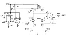
This circuit captures the PAR113 functionality. Select R8 for 200uA in the bias FET, use any decent rail to rail input modern dual, and the gain is just changed by a resistor across R3 and R2.
Attachments
Last edited:

Yes, it requires some dexterity & practice to place the part. For passives, it is easy, pick/move the part as it sits on the PCB. Put the part close to the pad area. The tweezers will bottom out against the PCB, insta cal, it really is quite simple, once you get the hang of it!! Lots of light req. I am fortunate in this regard, I am myopic Rick
I'm lucky to have an endless supply of just out of date syringes of solder paste. I have found those cheap USB microscopes from Taiwan are a great help. A drop on one lead and just tack it down, then go around and do the rest with some very thin solder.
Can someone please point me to the BF862 & J111 models that Guru Wurcer uses.
I've downloaded about 6 *.txt library files from this thread but can't seem to find the info in any of these.
I take it these are the favoured i/p devices/cascode.
I'm nearly at the stage of finalising a FET990. Gotta say I'm impressed by the original. Just adding the FETs as Scott has done is easy but keeping the supa dupa performance isn't. I think I've finally got something to rival the latest WurcerOPA 😀
Last edited:
.. and the 2sa970 & 2sc2240 too please?Can someone please point me to the BF862 & J111 models that Guru Wurcer uses.
ME= Mechanical Engineer. At least here in the States.
I thought perhaps Medical Examiner also, but i'm probably thinking of MD
I only miss the other output 😉
But I guess that it would be possible to use an OPamp "C" and use like like the B OPamp but on the left side of the LTP, right?
/S
But I guess that it would be possible to use an OPamp "C" and use like like the B OPamp but on the left side of the LTP, right?
/S
This circuit captures the PAR113 functionality. Select R8 for 200uA in the bias FET, use any decent rail to rail input modern dual, and the gain is just changed by a resistor across R3 and R2.
Here they are (BL-grade)
.MODEL 2SC2240 NPN (IS=99.13F XTI=3 EG=1.11 VAF=422.2 BF=352.8 ISE=1.179P
+ NE=1.782 IKF=.4704 NK=.9631 XTB=1.5 VAR=100 BR=1.663 ISC=555.1P
+ NC=1.796 IKR=5.85 RC=.2032 CJC=7.561P MJC=.2472 VJC=.3905 FC=.5
+ CJE=5P MJE=.3333 VJE=.75 TR=10N TF=1.295N ITF=1 XTF=0 VTF=10)
---------------
.MODEL 2SA970 PNP (IS=465.4F XTI=3 EG=1.11 VAF=57 BF=407.6 ISE=4.683P NE=2.051
+ IKF=.3998 NK=1.192 XTB=1.5 VAR=100 BR=1 ISC=465.4F NC=1.048
+ IKR=6.032 RC=2.343 CJC=11.59P MJC=.4014 VJC=1.155 FC=.5 CJE=5P
+ MJE=.3333 VJE=.75 TR=10N TF=1.252N ITF=1 XTF=0 VTF=10)
--------------
/S
.. and the 2sa970 & 2sc2240 too please?
I only miss the other output 😉
But I guess that it would be possible to use an OPamp "C" and use like like the B OPamp but on the left side of the LTP, right?
/S
Haven't tried that, there might be a common mode conflict. You could just invert the output to provide a minus half. The PAR 113 schematic on the web has the one side grounded on their differential input circuit. I have built this, it works quite well.
Scott, how do you feel about your rather flattering new Christian Name?
Just can't keep you Aussies down.🙂
Richard - I posted a zip file several days ago with all the models and a working FET input JE990.
Thanks for this Scott. I'll plead ignorance of the finer workings of LTspice. Indeed your zip has all I require.I posted a zip file several days ago with all the models and a working FET input JE990.
Gentlemen, it is a Title ! Please remember to genuflect as you say it unless you are on your knees as is right & proper. 🙂Scott, how do you feel about your rather flattering new Christian Name?
crap, heres me using the real name in my shorts? I suppose I will have no luck finding matched bf862 this weekend now... what can I do to make this right?
Can you beat this.... in the middle of the ocean there is wi-fi? I'm off the coast of southern Thailand... went to an island called Phuket and from there to a smaller island. And, they have wifi system here via mobile system. !
Question -- what is the reliable/accurate source of transistor parameters to use in SIM software?? Thx-RNM
Question -- what is the reliable/accurate source of transistor parameters to use in SIM software?? Thx-RNM
- Home
- Source & Line
- Analog Line Level
- Discrete Opamp Open Design