Fear of the technology being copied is a cover.
A firm like Hitachi buy all kind of chips , not only their own,
and i would be surprised that AD or other firms would refuse to
deliver accurate models if such a firm was to buy their products.
Disposal of accurate models is instrumental in reducing dramaticaly
designs costs as well as a time to market deadlines so the manufacturers
message is clear : buy our chips for significative $ amounts and you ll
get the good models , do otherwise and you ll soon be bankrupt...
I see. Keep the design models inhouse. Be involved in the design ... least one become just another $1B fab house. With that extra parts cost and a NDA one has business security. It works for awhile that way. Every stage of product development goes to a specialist.... sort of like the medical industry. Makes the books look good for stock holders. Its good for everyone but the end user who ends up spending more. There is a trend in Asia to be vertically intergated, though. Only last stage/fab farmed out.... sometimes.... with heavy stock investment in the fab/factories as well. Interesting times. We shall see.
It means we need to do some tests on our own for the parameters important to modelling audio designs. We dont need everything that an IC design team will come up with... just what is needed for accurate modelling for audio designs. What is needed then -- what are they and which ones are most often missing or not accurate? And, how are they measured? THX-RNMarsh
It means we need to do some tests on our own for the parameters important to modelling audio designs. We dont need everything that an IC design team will come up with... just what is needed for accurate modelling for audio designs. What is needed then -- what are they and which ones are most often missing or not accurate? And, how are they measured? THX-RNMarsh
Last edited:
Thanks for these Scott & Frank. My excuse is I'm new to dis internet stuff. 😱Gee Richard they are right there on the web site. This is the basis for them, http://www.analog.com/static/imported-files/application_notes/AN-138.pdf.
www.analog.com is indeed a treasure trove.
Dunhill, you might find their Analog Filter Wizard useful in your quest for the ultimate filter OPA.
OK. I give up. Is smarty-pants Wurcer going to tell us not-very-clever-unwashed-masses the answer?If you're very clever you can spot part of the problem in the credits.
I spent time in da old days, reducing Boyle models from the TI & Philips models so I could use them in my home brewed linear circuit analysis package. Was always disappointed to find how crude they were. Of course, I couldn't sim non-linear stuff but I trusted my own stuff for stability in dem days.
So it's likely the simplified models will give me exactly what I want. There's also a couple of ANs & tools on driving capacitive loads.
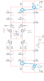
Is There An Error in Post 1568 Schematic?
I have been running LTSpice on the the topology shown in Post 1568. (Which I believe is the latest version.)
From looking at the circuit's gain-phase plots I think there may be a drafting error in the diagram posted at #1568. The secondary compensation pole-zero networks may be connected to the wrong sides of the differential input stages. See atch image "Post1568_Possible_Error.png".
I have also attached simulation result screen shots (and the native LTSpice files that generated them) showing the behavior of the Post 1568 circuit as-drawn. In particular, look at the unstable phase margin (MINUS 12 degrees) at the unity gain frequency.
Following posts will show results for modified versions of Post 1568. If the Post 1568 circuit topology should be modified to improve performance, I'd like to know because I'm laying out a PWB and don't have enough acreage to allow for compensation networks in BOTH locations!
Dale
Attachments
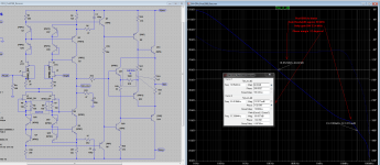
Corrected (??) Circuit from Post #1568
Here's how the performance improves when the compensation networks are placed on the other side of the input differential amps, and values adjusted for the higher values of emitter resistor. The low frequency gain-bandwidth isn't affected, but the unity gain phase margin improves considerably to PLUS 60 degrees. (The unity gain frequency decreases from around 33 MHz to about 13 MHz.)
Dale
Attachments
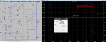
Tweaking Modified Compensation Scheme from Post 1568
And here is an example of what may be feasible with this circuit. It actually looks like a low-frequency gain-bandwidth of 50 MHz or more (with unity gain phase margin on the order of 30 degrees) might be practical without resorting to heroic efforts of selecting components, customizing each unit with the aid of a network analyzer, etc. (We started with an RF JFET, after all!)
By the way, I used the BC550/BC560 models from Bob Cordell for all of the BJT's in this sequence of simulations. I am quite aware that other models, and different component values, will give differences in specific result values - my major concern is determining where the compensation networks should be placed so I can proceed with the PWB layout.
Dale
Attachments

Here's how the performance improves when the compensation networks are placed on the other side of the input differential amps, and values adjusted for the higher values of emitter resistor. The low frequency gain-bandwidth isn't affected, but the unity gain phase margin improves considerably to PLUS 60 degrees. (The unity gain frequency decreases from around 33 MHz to about 13 MHz.)
Dale
I'll check tonight, it could depend on the particular device choice. Unity gain stability can be a tough issue and lots of small things can matter.
And here is an example of what may be feasible with this circuit.
Dale
They are correct for my device models, and in any case boosting VAS drive at high frequencies is what you want (the JE990 has a complex network here). I'm sure their values were empirical. I suggest that since as is at gains > 10 there is no problem you could fit short lines to each point and cut the unused one. I don't think the last word on unity gain operation will be until a good tight layout is exercised.
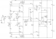
To summarize these are the values that ended up in my breadboard. I am showing them just to be exact there is certainly some latitude possible without changing much. The FET’s are 2SK170 cascoded by J310’s, the bipolar are all 2N4401/4403’s, the diodes 1N4148, bias set at 25mA total. I measured AOL and THD at 10Hz, 1KHz, and 20KHz. Everything looks good, damping the input and adding the 15pF made everything behave. The AOL at 10Hz was 400K and at frequency was right on simulation same for the third harmonics, everything above the thirds far down. Vos was 7mV (simulation of all perfectly matched devices was 3.8mV) with NO matching of any devices. This made for a slight increase of seconds over the sims, I’m sure matched devices and an offset trim would fix this. Yes these were all single devices pulled at random out of the bag.
Before I forget, thanks to EUVL, there is another useful JFET. The PMBFJ620 looks to be a dual high Vp BF862 type device, perfect for the cascode spot (I’m not sure the highish Vp works on the input devices). But a big heads up on another matched pair of low noise JFET’s with low capacitances (cheap, cheap too). Thank goodness for the emergency broadcast network.
I need to take a break on this for a while, we have a two week shutdown so I’m sure I will find time to do an SMT layout and I now have access to a reflow oven.
Attachments
PMBFJ620 is 6nV/sqrt device 🙁 I sent you samples several years ago 🙂PMBFJ620 looks to be a dual high Vp BF862
Nice part! And in a six pin package to boot. I think that information will be considered my holiday presentBefore I forget, thanks to EUVL, there is another useful JFET. The PMBFJ620 looks to be a dual high Vp BF862 type device, perfect for the cascode spot (I’m not sure the highish Vp works on the input devices). But a big heads up on another matched pair of low noise JFET’s with low capacitances (cheap, cheap too).

PMBFJ620 is 6nV/sqrt device 🙁 I sent you samples several years ago 🙂
I notice that noise is at 100Hz. I wonder how far below the corner that might be? If it were an ideal JFET the 10mS would represent about 1.05nV/sqrtHz.
Anyway, o.k. for cascoding.
PMBFJ620 is 6nV/sqrt device 🙁 I sent you samples several years ago 🙂
Dimitri, I'm sorry I forgot that it was you there is just so much stuff in my lab. Brad is right they are aimed at the AM car radio app and as such are probably close to the BF862 which if you look also has a fairly mundane datasheet spec.
Scott: Thanks so much! On your updated schematic, the two compensation capacitors in the center of the drawing (one 47pf to ground, the other value is blurred) Thanks, Ray😀
Brad, I suspect that they omit k in front of Hz. This JFET has three times less input capacitance and three times less transconductance than BF862I notice that noise is at 100Hz.
No worries, I'll remeasure it with condenser mike in mind 😀Dimitri, I'm sorry I forgot that it was you
Last edited:
Yes, I just grabbed two 47pF instead of 100pF no OCD behavior allowed 🙂.another 47pf
Thanks for this, Scott.... The FET’s are 2SK170 cascoded by J310’s ...
What current are you running in the i/p devices? It's not clear what J1 & J2 are?
Did you go for 2 x 5mA as on the previous versions?
Anyway, o.k. for cascoding.
PMBFJ620 was mentioned earlier in this thread as a dual J310 - if so, the Vds rating may be a bit low. I wonder if the J304 will work better for cascoding, with its 30V rating? No dual available, it seems.
A somewhat similar part is the old 2N5564 (-5, 6) dual, the process 96. Still made it seems. 40V breakdown, with National Semi databook showing a typical 55V for the process.PMBFJ620 was mentioned earlier in this thread as a dual J310 - if so, the Vds rating may be a bit low. I wonder if the J304 will work better for cascoding, with its 30V rating? No dual available, it seems.
Funny thing about that part was the version in an 8-pin DIP package with a different prefix, which looked like an opamp and was a little cheaper. I saw people sneer at boards, thinking that it was an opamp.
EDIT: NPD5564 etc.
Last edited:
- Home
- Source & Line
- Analog Line Level
- Discrete Opamp Open Design