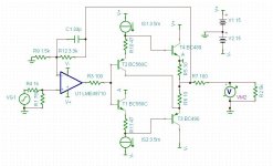
One mistake I realized when taking off the buffer was that I neglected to increase the value of the feedback resistors. So, I did that and it performs reasonably well in this configuration. I just multiplied the two resistors by 10. Distortion is 0.0007% driving a 5k ohm load at 1kHz, 1 Vp-p input, rising to 0.0009% @ 20kHz.
Oh shoot, I forgot to delete the 220pF capacitor. If I do that, bandwidth is fine with a smooth roll off starting at about 1MHz. I guess it's pretty obvious that the Miller capacitor's value is a function of the gain transistor, so in this case I was able to lower it to 5pF, and the distortion @ 20kHz went down a little to 0.0008%. Bandwidth rolls off at something like 10MHz with a 5pF capacitor.
Oh shoot, I forgot to delete the 220pF capacitor. If I do that, bandwidth is fine with a smooth roll off starting at about 1MHz. I guess it's pretty obvious that the Miller capacitor's value is a function of the gain transistor, so in this case I was able to lower it to 5pF, and the distortion @ 20kHz went down a little to 0.0008%. Bandwidth rolls off at something like 10MHz with a 5pF capacitor.
Attachments
Last edited:
Anyway, I cleaned the circuit up a little bit and this is where I'm at. It's probably usable as it is now.
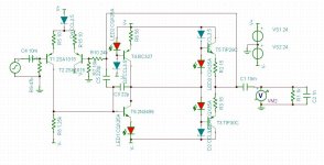
The specified VAS transistors for this board are the obsolete 2SD667/2SB647 complementary pair. They are listed as medium power transistors in the tall TO-92 package. Maximum power dissipation is 900mW, maximum current is 1ampere, and hfe is 100-200. I don't have spice models for these transistors so I substituted something similar.
And, just to be clear, I would not have been able to do this without the generous help of many people here on this message board. Thank you again for your clear guidance and support.
Attachments
Last edited:
Yes it's easy and IMHO a very good test to do!
Just short the input of the amp, apply the AC signal from the signal generator to the output of the amp through a 1Megohm resistor, and measure the AC voltage at the output of the amp.
The 1M resistor and the output impedance form a voltage divider, so it's easy to work out. E.g. If you apply 1V through a 1M resistor, and measure 1mV at the output, it means the output impedance is 1K. If you measure 0.2mV, it means the output impedance is 200R.
Why I like this is it gives an easy way to check stability into capacitive loads. With many/most amps, the output impedance rises at high frequencies. If the phase exceeds 90 degrees at any frequency, that means the amp will be unstable with some or other value of capacitive load. One AC sweep tells you all you need to know - easier than trial and error with various different capacitive loads.
You may also want to try with the input open circuit instead of shorted to earth as that may affect the result.
OK, I get 812mV. That's pretty bad...
It's also very sensitive to capacitive loads... sigh...
I think I have no choice but to add a buffer. I've tried several different kinds with this circuit. What's everyone's favorites? I'm looking for ideas... The single ended MOSFET looks like the most simple one so far.
Attachments
Last edited:
OK, I get 812mV. That's pretty bad...
It's also very sensitive to capacitive loads... sigh...
I think I have no choice but to add a buffer. I've tried several different kinds with this circuit. What's everyone's favorites? I'm looking for ideas... The single ended MOSFET looks like the most simple one so far.
Except for parts count/complexity your early "diamond buffer", although overkill, did have very good performance.
A MOSFET is probably fine as a buffer. The 2N6755 you have at the moment is an ancient power part in a big metal case, and has, owing to its chip size, a largish drain-gate capacitance, something else the second stage has to drive. The other thing about DMOS is to include a gate stopper resistor a la vacuum tubes, as they are prone to ~UHF parasitic oscillations without it, unless the trace run is tiny (and sometimes even certain package parasitics can be enough for RF oscillations; running at lower currents though, this is unlikely). If these are present you won't be able to see them with most 'scopes, but you'll note some very peculiar behavior as you touch portions of the circuit or even move your hands near it.
Note that although the DMOS gate-source C is quite large, except for absurdly heavy output loading (that your current source wouldn't support anyway), it is effectively bootstrapped out by the voltage follower action.
Brad
Ok, thanks. I just grabbed a mosfet. I didn't think twice about it. If I use one, it'll be a small one in a TO-92 package, like a 2N7000 or something.
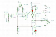
The alternative is to use the attached schematic, which is from another board I have on hand. All I did with it is to change a couple of resistors for CRD's and fooled with the feedback capacitor.
Attachments
Ok, thanks. I just grabbed a mosfet. I didn't think twice about it. If I use one, it'll be a small one in a TO-92 package, like a 2N7000 or something.
The alternative is to use the attached schematic, which is from another board I have on hand. All I did with it is to change a couple of resistors for CRD's and fooled with the feedback capacitor.
A 2N7000 would be fine, although a little close on breakdown voltage, and watch the dissipation. I use them a lot. Also a very old part (Siliconix IIRC promoted it as the "Fetlington", as a candidate to replace darlingtons for things like driving relays) but it's still a decent part for low capacitance and moderate transconductance.
Did you ever tell us why the +/- 32V rails? Although I have nothing against highish rails, these are just high enough to exclude a number of potential parts, despite there being plenty of 80V and up ones. Is it an existing power supply that drives this?
Oh, I don't know. That's just what the schematic calls for. We can make it any voltage at all since I haven't built any power supply for it yet. I just tried it at +/-15vdc and it's fine.
Thanks for the information and help!
Last edited:
No, that's not possible - something went wrong there.OK, I get 812mV. That's pretty bad...
It looks like you were measuring the DC offset voltage at the input of the amp. The idea is to measure the AC voltage at the output.
No, that's not possible - something went wrong there.
It looks like you were measuring the DC offset voltage at the input of the amp. The idea is to measure the AC voltage at the output.
Thanks. I'll look at it later. I think if I use the TIP29/TIP30 pair for the outputs, then it'll drive just about anything.
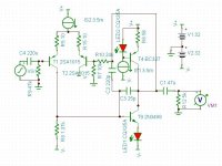
I think this one works very well. Distortion is 0.0008% driving a 1k ohm, 1nF load, with a 1kHz, 1Vp-p input. The outputs are running at about 40mA each. I changed to the standard +/-24VDC supplies used by professional audio. Bandwidth is good with a nice smooth roll off above 1MHz. I think this one is worth building.
I noticed a couple of errors in the circuit. I had changed the feedback resistors by a factor of 10, now I reduced them by 10 and distortion went down to 0.0004% under the same conditions, with bandwidth increased to beyond 1MHz.
I noticed a couple of errors in the circuit. I had changed the feedback resistors by a factor of 10, now I reduced them by 10 and distortion went down to 0.0004% under the same conditions, with bandwidth increased to beyond 1MHz.
Attachments
Last edited:
Also, just ignore the transistor types in the VAS. I don't have models for the 2SD667/2SB647 pair that belong in the real VAS.
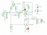
I'm tempted to build this one just to see the LED's light up... Ha, old tube guy here...
Distortion is still only 0.001% driving the 1kohm, 1nF load to 4.75vrms @ 20kHz. That's pretty good I think.
Oh, I was able to get spice models for the Central Semi CRD's. I'm using their 3.5mA model in the schematic.
Last edited:
What bias current are you passing through the output devices?
Could you adjust the output Re values to ensure that you have optimum ClassAB bias voltage and ClassA output current up to your desired limit?
Could you append the real component types to the schematic as a legend? Similarly for the CCS shown as Zener symbols.
Could you adjust the output Re values to ensure that you have optimum ClassAB bias voltage and ClassA output current up to your desired limit?
Could you append the real component types to the schematic as a legend? Similarly for the CCS shown as Zener symbols.
Last edited:
What bias current are you passing through the output devices?
Could you adjust the output Re values to ensure that you have optimum ClassAB bias voltage and ClassA output current up to your desired limit?
Could you append the real component types to the schematic as a legend? Similarly for the CCS shown as Zener symbols.
I mentioned it above. They have about 40mA each. These are TO-220 devices attached to heat sinks.
I don't know how to adjust the Re values to obtain optimum class AB bias voltage and class A output. I was just trying to get something to work well, using the software as a guide.
Well, I could add a BOM, but this isn't an ideal circuit, since I'm working off of an existing circuit board with it's own limitations. I wouldn't recommend building this, in other words, unless you were stuck with the same boards that I have.
The CRD I used is CCL3500:
http://www.centralsemi.com/PDFs/selection/leaded/CLD_Standard.pdf
Thanks for your interest.
Last edited:
I bias = 40mA.
Re = 15r
Vre = 40 * 15 = 600mVre
Optimum ClassAB bias voltage is ~26mV
Change Re to ~0r6 will result in Vre~24mVre
BUT ! How do you reduce the LED bias voltage so that the same 40mA passes through the output devices?
Two diodes may give ~1.25V, if you adjust the CRD current appropriately. Here a 3.5mA idss jFET might be better, then you adjust the source resistor to trim the output bias Vre.
The advantage of optimum bias is that the transition to higher output current than your maximum ClassA is delivered with minimal crossover distortion.
Last edited:
I bias = 40mA.
Re = 15r
Vre = 40 * 15 = 600mVre
Optimum ClassAB bias voltage is ~26mV
Change Re to ~0r6 will result in Vre~24mVre
BUT ! How do you reduce the LED bias voltage so that the same 40mA passes through the output devices?
OK, but changing the Re values only increases the current through the outputs without changing the bias arrangement. I tried changing to 6 ohms, but it just increased the output current to over 90mA, and the Vre was over 500mV. Distortion remained about the same as before with the same input.
I'm not expert enough to know what to do.
Thanks for your interest.
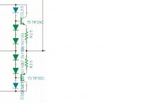
2 diodes giving ~1.2 to 1.3V instead of 2 LEDs giving 3.6V to 4V
OK, I changed it to the one shown, but it's no better in terms of distortion, though quiescent current is less. I tried just one diode per side, but couldn't get the transistors to conduct, even with a 5 ohm Re.
Attachments
I don't know what a 1n1183 is. Can you ask the simulator to tell you the voltage drop across each diode? And as a check, what the base to base voltage is of the output devices?
BTW, I am not expecting the ClassA performance to improve.
It's the transition to ClassAB that I am trying to help you with.
BTW, I am not expecting the ClassA performance to improve.
It's the transition to ClassAB that I am trying to help you with.
I don't know what a 1n1183 is. Can you ask the simulator to tell you the voltage drop across each diode? And as a check, what the base to base voltage is of the output devices?
BTW, I am not expecting the ClassA performance to improve.
It's the transition to ClassAB that I am trying to help you with.
Here's the diode spice file. I think it's just a normal small signal diode. Each diode has a 479mV drop across it.
The voltage at the base of the TIP29 is 3.95V, the voltage at the input junction is 2.99V, and the voltage at the base of the TIP30 is 2.04V. The output from the VAS is obviously not at 0VDC...
I could go back to the diamond buffer if that would perform better in your opinion.
Thanks for your help. Much appreciated!
Attachments
Last edited:
479mV is far to low. Either change the diode or increase the current. You need ~620mV across each diode to get the output bias current about right (40mA).
I cannot translate the spice model. I am not a simulator user. I do it with paper and pencil. When pencils become obsolete, I will be lost.
I cannot translate the spice model. I am not a simulator user. I do it with paper and pencil. When pencils become obsolete, I will be lost.
- Status
- Not open for further replies.
- Home
- Source & Line
- Analog Line Level
- discrete op amp