davesaudio said:All I could find on the polywhatsit
I looked at the assembly source file and found it most probably works as advertised. A couple of notes though.
It works at 8 bit resolution, what means roughly 48 dB of dynamic range and about the same (roughly) in terms of S/N ratio. This certainly fits well many applications such as practice amplifiers and similar, but falls rather short of the S/N acceptable for live performance or recording.
There is no attempt to process signals in the sense of scaling / mixing. It is limited to time delay, time reversal, pitch shifting and so on. Again this may be more than enough for many people. This is quite OK at 8 bits, for any further attempt to make calculations not only will probably exceed the speed capabilites of the processor, but also introduce round off errors, being each lost bit about a 6 dB loss in S/N.
As reference, consumer audio works at 16 bits, and DSP processing mandates a headroom of several extra bits to accomodate truncation. This is why usually 32 bit processors are called for this, better yet if they can handle floating point math.
Yet, this is truly a DSP example in the sense it works along the same basic philosophy.
On another line, I received today the TI samples (FIFOs, ADCs and DACs) and must now figure out how to handle 0.5 mm pin pitch devices
 !!!. Well, my big mouth put me here so I must find a way.
Most probably I will start with a delay building block comprising A/D, FIFO delay and DA. Once I have this in line I will combine them along the idea posted in the previous note. Will keep informed on progress.
Rodolfo
Ingrast, try this to handle the 0.5mm pin pitch: http://members.lycos.nl/anthonyvh/index.php?page=smd
I hope that helps! I'm eager to see results. I wish I could do things like this. Well, maybe in 3-5 years 😀.
I hope that helps! I'm eager to see results. I wish I could do things like this. Well, maybe in 3-5 years 😀.
SMD prototyping
Hey Devil_h@ck!
You've got excellent material there!! The soldering part I was not really worried about. The PCB manufacturing was, and your page I found excellent.
The process I use is slightly different, with bare copper clad and dry film hot pressed. I use soda ash developer and NaOH for stripping. Problem is it gets really hard to have good repetitive control of all parameters so as to have consistent quality fine resolution. The idea of using 2 piggybacked masks is cute! My Epson 1520 makes good artwork on transparency but much better on paper as you noted.
That you can get good SMD quality with basically the same tools is encouraging, will keep you informed.
Rodolfo
Ingrad, I'm glad that I can help a tiny bit 🙂. To get good control over the all the parameters, I suggest you try the silicate developper, it helps a lot when developping PCBs with tiny traces! If the traces are really small, I suggest you don't make the developing solution too concentrated, because even with the silicate developer it is still possible to overdevelop (but very hard), I've had it happen when I used 1 part silicate concentrate + 2 parts water (but there was something wrong with the PCBs themselves too) 🙂.
Digital delay progress update
I devoted some hours last weekend to work on the digital delay project.
Here is a draft design for the basic delay building block.
NOTE: This design is untested, being only the glue logic digitally
simulated to make sure no big blunder was lurking before committing to actual hardware construction. As such there may - most probably there are - undetected bugs to be found and corrected.
Brief description.
Process starts with conversion by U1, PCM1802 24 bit stereo A/D chip.
This device generates signals:
BCK: Clock signal for downstream devices to synchronize with data.
FSYNC:Frame synchronization signal, marks the beginning of a serial frame
LRCK: Left/right channel flag to indicate which one is being
outputted.
DOUT: Actual data stream.
The output stream is 24 bit I2S format selected by pins FMT0 and FMT1.
Timing is derived from a master clock running at 256x the sampling frequency. Varying the master clock between 8.19 and 24.57 MHz modifies the actual sampling rate from 32 ksamples/s to 96 ksamples/s, which in combination with a fixed 1024 or 4096 sample delay introduced by FIFO U2, yields the variable time delay.
DOUT is sent to the input of IC5/6 forming a 16 bit shift register. We settle to 16 bit actual word length to simplify hardware though U1 provides 24 bits and U2 can handle 18 bits.
LRCK and BCK are combined by IC1A to enable (EN_SHFT) the shift clock. Any one Low resets 4 bit counter IC2A to all zeros. IC3A detects the arrival of the 15th pulse (BIT15) and IC7A delays this signal a further period (BIT16) to enable shifting in the 16th most significant data bit. The delayed signal inhibits further shift clock pulses, freezing IC5/6 to present a parallel 16 bit word corresponding to the A/D most significant 16 output bits. IC7B delays BIT16 a further clock period to accommodate a gating signal for writing the FIFO.
FIFO writing is accomplished by pulling down input WEN to which end the inverted combination of FSYNC and LRCK (IC11A) comes handy. Output of gate IC8B (WCLK) is a negative going half cycle of BCK, in whose rising edge data is actually written to U2.
For the first 1024 or 4096 frames, the FIFO fills up with data until it becomes full. Output FF goes low once the last available storage position is filled, and we gate an inverted BCK half cycle with FF (IC11B/C) to generate RCLK. On the positive transition of RCLK, the word written 1024 or 4096 frames back is outputted by U2, while this very read operation frees one place thus rising the FF signal back to idle (High). From here on, FF cycles once each audio frame.
Signal LRCK comes handy to gate the FIFO output word into IC8/9 forming a parallel load shift register, we use the same BCK for shifting. When LRCK goes up, IC8/9 latch the 16 bit word and begin shifting it out. The shift register cascade serial input is grounded, so after the first 16 bits just read from the FIFO are shifted out, zeroes follow for the D/A to read, emulating zero value bits up to the 24th it expects. The clock may be left running, for the D/A takes care for itself once it has read the needed bits. A multiplexer might have been used here instead of the
shift register with the same effect for serializing with a little
different logic, probably a bit simpler but I had already ordered the S/R's so this is it for the time being.
The DSD1791 24 bit stereo D/A converter is a complex chip programmable through a serial control interface. Fortunately it is designed to operate stand alone with reasonable defaults, one of which is the I2S 24 bit data format. It is driven by the same BCK, LRCK and FSYNC signals generated by U1, only it uses delayed input data for conversion.
Master clock generator details have not yet been worked out, but I plan to use a TLC2932 PLL which provides a control range adequate for varying the frequency from 8.19 to 24.57 MHz as required. Superimposing a low frequency signal on the control voltage will provide sort of tremolo effect.
Since both the A/D and D/A are stereo chips, I plan to use one half of each for a long 4096 stage delay and for a shorter 1024 stage one.
Right now I will focus on manufacture of carrier boards for the smallest SMD devices. This carrier boards will have DIP style rows of .1 pitch holes to make is easier for the motherboard to design and construct.
All devices are available as free samples from Texas Instruments. I highly recommend to register there if you are interested in building prototype systems like this.
Will keep posted (hopefully with photographs) of further advances.
Rodolfo
Attachments
Project goings
I managed to devote some hours last weekend to the project, here are the reults so far.
I tried with encouraging results fabrication of fine line carrier boards for the smallest SMD's. I am confident with some time I will have the little beasts tamed enough to build the prototype.
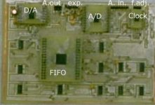
I finished the basic module design, here is the schematic for one delay block and A/D - D/A conversion. the next post is the PCB, which I designed as single sided with lots of vertical jumpers and that can be latter converted to double sided.
This module includes conversion, FIFO and clocking. Provision for a second delay module is included in expansion connector SV3 to export and import the second audio channel generated / received from the stereo A/D - D/A chips.
Connector SV1 provides access to plug a pot (10k is fine) for clock speed adjustment.
SV2 is the audio input and SV4 the output. Separate +3.3 VCC, +5 and -5V must be supplied as well as separate digital and analog grounds.
This module should be integrated with an analog one where actual combination of signals is performed.
Hope to build it next week or the other, will keep posted.
Rodolfo
I managed to devote some hours last weekend to the project, here are the reults so far.
I tried with encouraging results fabrication of fine line carrier boards for the smallest SMD's. I am confident with some time I will have the little beasts tamed enough to build the prototype.
I finished the basic module design, here is the schematic for one delay block and A/D - D/A conversion. the next post is the PCB, which I designed as single sided with lots of vertical jumpers and that can be latter converted to double sided.
This module includes conversion, FIFO and clocking. Provision for a second delay module is included in expansion connector SV3 to export and import the second audio channel generated / received from the stereo A/D - D/A chips.
Connector SV1 provides access to plug a pot (10k is fine) for clock speed adjustment.
SV2 is the audio input and SV4 the output. Separate +3.3 VCC, +5 and -5V must be supplied as well as separate digital and analog grounds.
This module should be integrated with an analog one where actual combination of signals is performed.
Hope to build it next week or the other, will keep posted.
Rodolfo
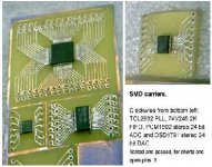
Progress report
Apologies for the poor images, the camera on hand does not focus closeup and I had to hold a magnifier glass in front to barely snap something.
SMD carriers are ready and devices soldered and tested OK.
Will now build mainboard.
Rodolfo
Apologies for the poor images, the camera on hand does not focus closeup and I had to hold a magnifier glass in front to barely snap something.
SMD carriers are ready and devices soldered and tested OK.
Will now build mainboard.
Rodolfo
Attachments
Yes, there is where DSP shines. In this case (don't know details of Audigy card) probably with a mix of on board processing as well as host (PC CPU) processing.
Rodolfo
Rodolfo
The dsp on the sound card does 100% of the sound processing, and the cpu just runs the user interface for making changes. The user interface can even be closed and the card will continue to run it's code. There is no load sharing required, this is how I can run a six channel active xover with time delays and parametric eq and still make 3d cad solid models with the music playing. Someday when I can afford it I will make a home theatre from this pc.
PC based audio processing
Some years back I thought the emerging paradigm should be the PC based audio machine.
Now I am somewhat backtracking from that idea, I do not see a solid trend in this direction. May be PC's are not solid and reliable enough - not even too practical - except of course for more or less techno geeks as we ourselves in a way are.
That is, the PC does not look much as an appliance but perhaps for regularly identified jobs like Internet / e-mail.
May be I am wrong, but I feel the PC - capable as it should be for the job - will not storm neither the home theater segment nor the professional stage audio management. I mean, not that it is not used, but that it is not mainstream.
Rodolfo
Ingrast, I agree completely with you that the pc is not suitable for mainstream audio. We techno geeks can have variable degrees of success and satisfaction from specialized applications of the pc by being careful, but it is still an experimental system, responding to the hand of it's builder. Perhaps the pc can be thought of as an emulator, which may function well but is constrained to stay in the laboratory. The knowledge gained by using the audio pc is valuable and achieved at minimal cost (important factor for hobbyists with growing families) but to set it free of the lab it must be implemented by more portable and robust means. So keep up your good work!
Digital delay progress
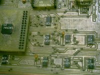
After some weeks pulling time to work on the project, the basic module is mostly assembled except for the output current to voltage converter.
Power has not been applied yet, so the magic smoke allways packed inside each electronic component has not been released😀
Apologies for the phono quality, will try to upgrade to a better camera soon.
Attachments
- Status
- Not open for further replies.
- Home
- Source & Line
- Digital Line Level
- digital reverb or delay