Hi,
Hi,
I've managed to get THD for the basic UCD design down alot more as well (4.X E-02), Power went out last night though so I couldn't finish what I was doing.
It seems shoot through on it is now much worse than it once was for reasons unknown, it can be reduced significantly by increasing Ron to 50 ohms, which is not useable, along with adding a fair bit of dead time.
I will simply not worry about it at all since this is modelled so poorly, but it's interesting to know there's over +-100amps shoot through in the simulation.
Regarding the PCB, the drivers seem to like a low impedance /high current path, to bring THD down anyway, the floating outputs like more current, which seems to bring up to 500mW! Provisions on the PCB to heatsink those somehow as well might be good.
For some reason the Bode plots I did looked inverted, with phase starting at 180 deg. and eventually crossing zero, and gain being negative, which could sort of make sense but, the amp isn't wired in an inverting configuration? That was for the differential input version anway, I'll post a few circuits as soon as possible but I wont' have much time to work on it today.
Johan do you have an alternative circuit for the precharge of the bootstrap circuit?
I think it's a great idea to offer a few options, might be easiest to make the output modular as mentioned before, than we only need 1 pcb for 1 half bridge and they can do anything they like with it. Most of the other circuit options you mentioned I think should be nailed down ahead of time, people, including myself, won't want to have to play with pcb layout to get it going, alot might not be able to do it properly either.
They are fun options to play with, but we did provide them with working sims to do that with, so I think unless it has to do with provisions for new feedback loops or going full bridge, the design should be nailed right down, should also allow you to make a simpler and more robust pcb that will work the same way for everybody, they'll have the Eagle file if they want to try something new they've simulated anyway. Sorry I couldnt' tell from looking at it, or missed it if you said so already, are you going with a ground plane layer?
Regards,
Chris
Where exactly (in which component(s)) do you mean those 500mW is dissipated? Could you elaborate how that might be a concern in the pcb layout?classd4sure said:Regarding the PCB, the drivers seem to like a low impedance /high current path, to bring THD down anyway, the floating outputs like more current, which seems to bring up to 500mW! Provisions on the PCB to heatsink those somehow as well might be good.
Johan do you have an alternative circuit for the precharge of the bootstrap circuit?
I think it's a great idea to offer a few options, might be easiest to make the output modular as mentioned before, than we only need 1 pcb for 1 half bridge and they can do anything they like with it. Most of the other circuit options you mentioned I think should be nailed down ahead of time, people, including myself, won't want to have to play with pcb layout to get it going, alot might not be able to do it properly either.
They are fun options to play with, but we did provide them with working sims to do that with, so I think unless it has to do with provisions for new feedback loops or going full bridge, the design should be nailed right down, should also allow you to make a simpler and more robust pcb that will work the same way for everybody, they'll have the Eagle file if they want to try something new they've simulated anyway. Sorry I couldnt' tell from looking at it, or missed it if you said so already, are you going with a ground plane layer?
No, I don't have a precharge circuit alternative right now; I though that could be a common part one could place with startup/shutdown logic on a separate board (perhaps together with a power supply). That's another small project 🙂.
I think I will continue work on an all-options board design, it's easier (for me) to nail down options from there later to produce a stripped-down layout on request.
And yes, the upper side should be mostly ground plane, and all left-over space on the bottom will be ground too...
Cheers / Johan
Bruno wrote:
My question is: Do you care about the reverse-conduction during dead-time at all ? My imagination tells me that it leads to losses in the recovering body diode AND in the FET that is switching on. But how severe are they when "normal" FETs are used ? I know that there are MOSFETS with built-in Schottky diode but you usually don't get these just around the corner.
Regards
Charles
Depending on the magnitude of the current, the body diode will have been in conduction during the dead time or even during the full cycle (=when the voltage drop across Ron exceeds 1Vf).
My question is: Do you care about the reverse-conduction during dead-time at all ? My imagination tells me that it leads to losses in the recovering body diode AND in the FET that is switching on. But how severe are they when "normal" FETs are used ? I know that there are MOSFETS with built-in Schottky diode but you usually don't get these just around the corner.
Regards
Charles
johanps said:
No, I don't have a precharge circuit alternative right now; I though that could be a common part one could place with startup/shutdown logic on a separate board (perhaps together with a power supply). That's another small project 🙂.
I think I will continue work on an all-options board design, it's easier (for me) to nail down options from there later to produce a stripped-down layout on request.
And yes, the upper side should be mostly ground plane, and all left-over space on the bottom will be ground too...
Cheers / Johan
Hi,
Where exactly (in which component(s)) do you mean those 500mW is dissipated? Could you elaborate how that might be a concern in the pcb layout?
It seems to work best with the floating comparator outputs running on the hot side, concern for pcb to arrange for possible heatsinking? Looks like they might need it, but when trying to optimise I seem to find strong interactions with most of all other values, so it might be possible to optimise while keeping those cool, not sure yet.
I though that could be a common part one could place with startup/shutdown logic on a separate board (perhaps together with a power supply). That's another small project 🙂.
Sounds good.
I think I will continue work on an all-options board design, it's easier (for me) to nail down options from there later to produce a stripped-down layout on request.
Whatever is easiest.
Right on.
Regards,
Chris
phase_accurate said:Bruno wrote:
My question is: Do you care about the reverse-conduction during dead-time at all ? My imagination tells me that it leads to losses in the recovering body diode AND in the FET that is switching on. But how severe are they when "normal" FETs are used ? I know that there are MOSFETS with built-in Schottky diode but you usually don't get these just around the corner.
Regards
Charles
I hear ya, I'm impressed enough the models seem to switch decently at all, I think I'll be thankfull for that and leave it right there. We'll find out when someone builds it..
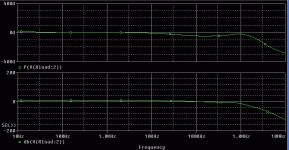
Honestly, right now I'm lost with Bode plots. It's not looking at all like I think it should, though I could be wrong.
In a non inverting type, to the patent design, phase is starting at 180 degrees, doesn't reverse until 800 or 900khz!, and gain is negative? Gain looks normal if divided by the input, but it should be doing that anyway. Can someone help me make sense of this please?
Regards,
Chris
Hi,
Can anyone comment on the above? Otherwise I'm giving up on it. Value changes in the feedback network do nothing to the gain/phase, gain is showing as negative yet isn't possible, when it produces +50W at 1 volt input, gain can't be negative, and why is the phase starting at 180 deg, when it isn't in an inverting configuration.
I've loaded one of my first schematics and did the same, its' an identical circuit with different parts. Gain showed up properly, but the rest is still the same, looks like it should be oscillating at 900Khz. I've tried every Bode graphing option I found for orcad and all results look the same, even with taking it from within the feedback loop, out of desperation.
Is it correct and I'm simply looking at it wrong? Seriously it's got me lost, which isn't good since that's the heart of this amplifier.
Thanks
Hi Chris,
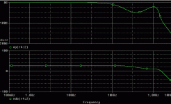
I can't help you much to make heads or tails of your strange bode plots. Attached is what I got out of an AC analysis on the ucd_js2 circuit which I posted a while ago. It should be equivalent to yours I believe. My plot looks "sane", but I wouldn't trust it too much since it deviates somewhat from the theoretical curve I got by analysing the filter equations with gnuplot eariler....
Regards / Johan.
Attachments
Hi Chris,
your schematic will not work for AC analysis. You might take a look at the Distortions in class D thread, or google for average switching stage model, state space averaging, Middlebrook and Cuk articles, Ray Ridley models and articles, Intusoft newsletters,
Unitrode design seminars, etc. You will find enough information about AC modelling of switch mode power supplies that can be directly applicable to class D amplifiers. When I will have some more time I will try to post some links or even some averaged spice models.
Best regards,
Jaka Racman
Hi,
Thanks for the replies on that guys.
Johan your plots are right on mark as far as what I envisioned I "should" be seeing out of them. Was that from the basic UCD circuit as well? What is bothering me is I at least got plots that looked just like that with my very first UCD simulation.
Hi Jaka, interesting and reassuring, because it didn't seem to work at all! Then again I look at Johan's plots now and ???
Heh. I realize they likely won't be fully accurate or anything, I would however be content if it made sense a little bit.
I think I'm going to post my differential circuit tonight, it's gone through a few more minor changes, I still haven't tried it with ideal switches and I would like to. I also promissed a try at a full bridge version so I'll have to get to work on that as soon as I post the updated differential.
Just going to run a slew of tests on it first to make sure it doesnt' do anything like start clipping at certain frequencies like that last one did 🙁 Also necessary because I did get a tad creative last night, and made an addition which helped the THD a fair amount, but it's only been tested at 20khz so far. AC analysis would have been nice for that.
Anyway thanks again for replying on that, it seemed like a silly question to be asking but I guess it wasn't, and now I at least have an avenue to investigate. Though I truly am perplexed why johans look like mine used to and dont' anymore. As I think I had said before going back and making the same plot of the first simulation circuit I had no longer looks the way it used to either, actually Orcad has been a bit strange lately, maybe I should re instal it. (sometimes the same circuit doesn't simulate the same way twice) and it did lock my last project. hmmm
Regards,
Chris
Hi,
This isn't the circuit, just a bode plot of my first working sim of a UCD. You can see it looks nothing at all like the last I posted, it looks exactly like what Johan posted, and makes alot more sense, even though it's wrong also. Sometimes it's good to question the old software but I still have a tendency to question myself first, always will.
The curious thing is simulating your Js2 Johan, the results dont' look like these, but like the previous ones I posted. I can't even pretend to understand what's going on with it
Suffit it to say Jaka Racman was more than right, it can't be done, not with this kind of a setup anyway. What a shame, but I'm happy to know the fault isn't my own, whatever it is.
Thanks,
Chris
Attachments
Hi Chris,
to get meaningful Bode plots from shematic that is suitable for transient analysis must be purely coincidental. Spice normaly determines DC operating point of the circut and then applies small signal AC analysis around this point. In shematic like yours this would almost inevitably be with one mosfet fully on and another one off.
I was looking for Unitrode app note that actually shows how to derive averaged spice models, but I could not find it. But this link and this link might show you what was I thinking about. If you find model for synchronous buck converer, you will be fine. (synchronous buck converter is SMPS talk for class D halfbridge output stage.)
Best regards,
Jaka Racman
Hi,
Yeah I've looked into state space modelling before when I realized syncronous converters were what I was after, but have to admit the information I've found on state space modelling just isn't geared towards someone of my level, I'll certainly check out your links though, many thanks.
I was under the impression it was done because spice was unable to perform the high speed switching, when I saw it appeared to do that OK, I thought there was no reason why it shouldn't give half decent AC results, apperently in error.
Also your explanation of coincidental (semi) meaningful Bode plots in this case is certainly in agreement with the results I've been getting.
So, seems I've learnt something new, it hurts and I'm going to go sit down 🙂
Regards,
Chris
Hi,
Here is the updated version, you'll see a "coupling cap" I placed on the input to bypass switching noise, simulations seem to like it, at high frequencies.
Switching frequency is certainly on the high side, why? Because I tried to increase the gain of the feedback network by lowering the resistance in series with the cap. It isn't the proper way of doing it, but it makes a remarkable difference. There's next to no visible ripple on the output at any frequency or power level. Might be worth running some hot mosfets for that.. I included a few screenshots, one showing variation of switching frequency, one of the circuit, the *.DSN file itself is also included.
Here's some results:
Fs=725khz
All 5 harmonics, R52=10
____________
.1 volt, 1khz
DC COMPONENT = 1.404313E-02
TOTAL HARMONIC DISTORTION = 1.449520E-02 PERCENT
_____
.1volt, 20khz
DC COMPONENT = 1.445609E-02
TOTAL HARMONIC DISTORTION = 5.303042E-02 PERCENT
____________
1volt, 1khz
DC COMPONENT = 2.225529E-02
TOTAL HARMONIC DISTORTION = 1.655159E-01
_____
1 volt, 20khz
DC COMPONENT = 1.406940E-02
TOTAL HARMONIC DISTORTION = 2.243623E-02 PERCENT
_______________________________________________
Feedback welcome.
Regards,
Chris
Ugh, I did it again, Here's the file. (I blame the heat)
Ok it seems that it isn't doing a great job compressing this time. All I'm including therefore is the circuit screenshot and the design file, I already posted the results anyway, should be enough to peak your interest.
For anyone who wants to simulate it, create a new orcad project with all libraries added, open the design file, copy and paste it into your new project, replace any parts that give errors with equivalents from your own libraries. Easiest way I found.
Regards,
Chris
Attachments
Hi,
So I've been playing with a full bridge version..
It works for a few cycles of the input, than both half bridges seem to fall out of synch, one might float high the other reverses, it might start switching again for a short time.
I think the problem lies with the feedback, for some reason its' oscillating at least twice as fast as the input signal.
That could be another problem altogether of course. All I did was mirror what's there, set the filter's inductor values to half what they were, and added a coupling cap, tried a few values for it.
The circuit is just a rats nest right now so I won't post it, but if anyone has any ideas as to what I should look for, I'd certainly appreciate it.
The comparator outputs work as expected anyway so that's good.
Regards,
Chris
Removing the squeak and the pop ...
Hello
I had a little problem with my soda (Self Oscilating class D Amp).
Ok this thread is about the ucd but but i wanna ask something about a problem that is described already in this thread which can happen in ucd and soda.
For the ones who don't know what soda is, you can see the principle in the next picture i found in another thread on the forum:

As far as i know, they make a "power astable multivibrator" and then they put a LP filter behind it. (filter is not in picture)
So you get a class d amp, of course the ucd will be better, because it takes feedback behind the filter instead of at the switches (soda), but i made a soda as DIY project for school.
The problem is:
This is the same in soda.
The solution was also already said:
Ok, this is so when you use the discrete comparator from ucd.
But i used a LM311 in my soda.
Bruno Putzeys said the same about his sodas in another thread:
Now you know, there is no discrete comparator in soda.
Thats why i wanna ask, can i use the "strobe" pin on the LM311 to solve the problem?
I thought so because the datasheet told me that u can disable the output with the strobe pin.
So can i avoid a squeak and a pop with using the strobe pin? And if someone maybe knows how, can you tell it?
What you people think about this?
A little picture of the "strobe configuration" in the next datasheet on the first page:
http://cache.national.com/ds/LM/LM111.pdf
Greetz
Bart
Hello
I had a little problem with my soda (Self Oscilating class D Amp).
Ok this thread is about the ucd but but i wanna ask something about a problem that is described already in this thread which can happen in ucd and soda.
For the ones who don't know what soda is, you can see the principle in the next picture i found in another thread on the forum:
As far as i know, they make a "power astable multivibrator" and then they put a LP filter behind it. (filter is not in picture)
So you get a class d amp, of course the ucd will be better, because it takes feedback behind the filter instead of at the switches (soda), but i made a soda as DIY project for school.
The problem is:
Allowing the PSU to run out on a UcD circuit will not produce any damaging pulses. It will not be very clean either (a squeak and a pop).
This is the same in soda.
The solution was also already said:
Use the current source to turn it off before that happens.
Ok, this is so when you use the discrete comparator from ucd.
But i used a LM311 in my soda.
Bruno Putzeys said the same about his sodas in another thread:
(for information to the other readers, soda typically used an LM311 comparator, an emitter follower pair as driver, ac coupling with zener DC restoration and a P/N pair. Needless to say startup of this circuit was a bit tricky)
Now you know, there is no discrete comparator in soda.
Thats why i wanna ask, can i use the "strobe" pin on the LM311 to solve the problem?
I thought so because the datasheet told me that u can disable the output with the strobe pin.
So can i avoid a squeak and a pop with using the strobe pin? And if someone maybe knows how, can you tell it?
What you people think about this?
A little picture of the "strobe configuration" in the next datasheet on the first page:
http://cache.national.com/ds/LM/LM111.pdf
Greetz
Bart
Hi El Burto,
It is, but I guess perhaps not in the original one. The later version had feedback both before and after the filter.
If your strobe pin can disable the comparator I guess it should work ok.
If memory serves me, there was an input buffer feeding the comparator, having a very elegant N channel pull down as a "Mute" feature at the input of the buffer. Could this serve your purpose as well?
Regards,
Chris
As far as i know, they make a "power astable multivibrator" and then they put a LP filter behind it. (filter is not in picture)
It is, but I guess perhaps not in the original one. The later version had feedback both before and after the filter.
If your strobe pin can disable the comparator I guess it should work ok.
If memory serves me, there was an input buffer feeding the comparator, having a very elegant N channel pull down as a "Mute" feature at the input of the buffer. Could this serve your purpose as well?
Regards,
Chris
Hi,
IMHO, pulling down the strobe pin gives you maximal DC on output, of course, if am i correctly imagine your driver.
IMHO, pulling down the strobe pin gives you maximal DC on output, of course, if am i correctly imagine your driver.
- Status
- Not open for further replies.
- Home
- Amplifiers
- Class D
- Development of a "reference" class D starting point