Hi
Great !, that looks like the expected result.
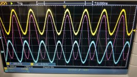
Pink trace is what see the load resistor, this is the signal the loudspeaker will see, then the music you want to hear... : that's the useful signal.
Amplitude is twice amplitude of each output, which is exactly what we expect from a BTL configuration.
Why doing this ?
Now you can hide channel 1 and channel 2 in order to only get on screen pink trace ( ch1-ch2), then repeat your measurement in post #365 : magnify the signal in order to display and measure the residual 600kHz ripple. Then you will be able to compare it with the useful signal (1kHz sine wave) and calculate the ripple ratio with some easy math.
But without doing math, the scope shows that the pink trace is less noisy than the yellow and the blue. As the two class D amp connected to Vout- and Vout+ are synchronous, the 600kHz ripple is synchronous too and the difference of the two signal cancel the ripple. Which should leads you to the conclusion that additional filtering is not necessary.
I'll try to measure on my setup (still a prototype ...) and report later.
Chris
Great !, that looks like the expected result.
Pink trace is what see the load resistor, this is the signal the loudspeaker will see, then the music you want to hear... : that's the useful signal.
Amplitude is twice amplitude of each output, which is exactly what we expect from a BTL configuration.
Why doing this ?
Now you can hide channel 1 and channel 2 in order to only get on screen pink trace ( ch1-ch2), then repeat your measurement in post #365 : magnify the signal in order to display and measure the residual 600kHz ripple. Then you will be able to compare it with the useful signal (1kHz sine wave) and calculate the ripple ratio with some easy math.
But without doing math, the scope shows that the pink trace is less noisy than the yellow and the blue. As the two class D amp connected to Vout- and Vout+ are synchronous, the 600kHz ripple is synchronous too and the difference of the two signal cancel the ripple. Which should leads you to the conclusion that additional filtering is not necessary.
I'll try to measure on my setup (still a prototype ...) and report later.
Chris
Hello AIM65,
Thank you for teaching me how to test the CLASS-D signal.
I will hide the CH1 and CH2 waveform and check the status of the differential signal in detail.
These two days are my holidays.
I will update the status next week.
Thank you again.
Thank you for teaching me how to test the CLASS-D signal.
I will hide the CH1 and CH2 waveform and check the status of the differential signal in detail.
These two days are my holidays.
I will update the status next week.
Thank you again.
Hi Knee266,
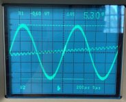
This i what I get.
First trace @200us/div time base shows 1kHz signal on output resistor (8Ω) with 5.3Vpp.
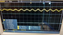
Second trace @5us/div time base shows same signal but highlight the 600kHz part with approximatively 200mVpp. Not null, but ok.
Chris
This i what I get.
First trace @200us/div time base shows 1kHz signal on output resistor (8Ω) with 5.3Vpp.
Second trace @5us/div time base shows same signal but highlight the 600kHz part with approximatively 200mVpp. Not null, but ok.
Chris
Attachments
Hello AIM65,
It seems that my oscilloscope can’t turn off the CH1 and CH2 display.
The 600KHz carrier on my board has not disappeared completely, same as your test result.
The amplitude of the carrier will increase as the volume increases.
Thank you.
It seems that my oscilloscope can’t turn off the CH1 and CH2 display.
The 600KHz carrier on my board has not disappeared completely, same as your test result.
The amplitude of the carrier will increase as the volume increases.
Thank you.
As the LC-filter has a fixed damping at 600 kHz it is not surprising, that the ripple will increase with the volume...The amplitude of the carrier will increase as the volume increases.
As said: calc the damping in dB to verify the output filter.
Hello MKSounds,
This is a CLASS-D feature, and it is not necessary to filter out this ripple, as suggested by AIM65.
I don’t know if it will affect the sound quality, but I will try it, if I can reduce this ripple.
Thank you.
This is a CLASS-D feature, and it is not necessary to filter out this ripple, as suggested by AIM65.
I don’t know if it will affect the sound quality, but I will try it, if I can reduce this ripple.
Thank you.
Project status & how to proceed
Hello, my first post on this forum with (apologies in advance) a bunch of questions.
If I understand correctly from reading the forum, you have been successful in implementing the TAS3251 hardware and software using a kicad design based upon the TI evaluation kit. Congratulations to all, it's a remarkable achievement! I understand your design is non-commercial open source for DIY. Further, there will be no more boards available for purchase from the original project instigators. For those thinking of getting involved, could I ask:
Thanks
Paul
Hello, my first post on this forum with (apologies in advance) a bunch of questions.
If I understand correctly from reading the forum, you have been successful in implementing the TAS3251 hardware and software using a kicad design based upon the TI evaluation kit. Congratulations to all, it's a remarkable achievement! I understand your design is non-commercial open source for DIY. Further, there will be no more boards available for purchase from the original project instigators. For those thinking of getting involved, could I ask:
Where are the kicad source files? I don't see them on either GitHub, only PDF schematics, nor have I found them on the forum by several keyword searches.
Has the performance of the final design been measured? (Power, noise, THD, IHD)
A list of required equipment would be great. I guess a hot-air soldering station as a minimum. Eg, do you consider it necessary to have an oscilloscope for debugging?
I understand the TI data sheets have many errors. Has a list of corrections been produced? Has TI been informed of these errors?
Thanks
Paul
Last edited:
After I using the second L/C filter, the 600KHz carrier amplitude almost disappeared.
But I saw the resonance frequency(70KHz @42mVpp~100mVpp) of the first LC and other carriers on 7xKHz waveform.
Does CLASS D really contain so many frequencies?
Thanks,
But I saw the resonance frequency(70KHz @42mVpp~100mVpp) of the first LC and other carriers on 7xKHz waveform.
Does CLASS D really contain so many frequencies?
Thanks,
Attachments
Last edited:
Hello, my first post on this forum with (apologies in advance) a bunch of questions.
If I understand correctly from reading the forum, you have been successful in implementing the TAS3251 hardware and software using a kicad design based upon the TI evaluation kit. Congratulations to all, it's a remarkable achievement! I understand your design is non-commercial open source for DIY. Further, there will be no more boards available for purchase from the original project instigators. For those thinking of getting involved, could I ask:
- Where are the kicad source files? I don't see them on either GitHub, only PDF schematics, nor have I found them on the forum by several keyword searches.
- Has the performance of the final design been measured? (Power, noise, THD, IHD)
- A list of required equipment would be great. I guess a hot-air soldering station as a minimum. Eg, do you consider it necessary to have an oscilloscope for debugging?
- I understand the TI data sheets have many errors. Has a list of corrections been produced? Has TI been informed of these errors?
Hi Paul,
- I have one board left and also some parts.
- I have no measurement available, maybe JMF11 does, same for pcb files.
- Hot air gun is not mandatory, to solder the TAS3251 may be a bit tricky, but with a good iron, good solder wick, leaded solder and some training, this should be alright.
- TI knows about data sheet quality.
- During the software design process I encounter many data sheet error, but some workarounds have always been found.
Chris
Hello Paul,
To answer your questions:
They have not been so responsive either on TI e2e website. AIM65 did a really good job to identify some workaround to tricky issues.
All in all, I think that this board is a "perfect" module for active speakers in a digital system, combining I2S input, DSP, DAC and TPA3251 power stage.
There is no commercial intention, and objective is to make available something with good quality components, that would allow easy tweaking to fit exact neeeds: easily change caps and selfs to adjust to speaker impedance, or personal tastes.
To complement AIM65 proposal, there are still 2 partially populated boards available for experiments.
To answer your questions:
- Where are the kicad source files? I don't see them on either GitHub, only PDF schematics, nor have I found them on the forum by several keyword searches.
- Has the performance of the final design been measured? (Power, noise, THD, IHD)
- A list of required equipment would be great. I guess a hot-air soldering station as a minimum. Eg, do you consider it necessary to have an oscilloscope for debugging?
- I understand the TI data sheets have many errors. Has a list of corrections been produced? Has TI been informed of these errors?
They have not been so responsive either on TI e2e website. AIM65 did a really good job to identify some workaround to tricky issues.
All in all, I think that this board is a "perfect" module for active speakers in a digital system, combining I2S input, DSP, DAC and TPA3251 power stage.
There is no commercial intention, and objective is to make available something with good quality components, that would allow easy tweaking to fit exact neeeds: easily change caps and selfs to adjust to speaker impedance, or personal tastes.
To complement AIM65 proposal, there are still 2 partially populated boards available for experiments.
Hi Chris
Thanks for your response. One board might be good for practice, but not so much for stereo crossover. I guess the quality of this would be fine for my ears, having experienced only low end hifi / upper end consumer grade but am looking at this as an interesting project to fit out a listening room for retirement. Still I want the best I can get without spending a fortune. I'm currently experimenting with DIY panel speakers, so looking for the simplest solution for building digital crossover and eq. I've not done any DIY hifi before now, but have programming skills and enough of a background in electronics (training but no practical experience) to follow documentation etc.
Catching up on what's available in hifi just recently after many years, I was surprised that multi-channel 'all digital' amp / filter systems seem to be still a rarity. Surprised for example that home theatre systems don't cater for it, given that they already have the requisite machinery inside the box.
Paul
Last edited:
All in all, I think that this board is a "perfect" module for active speakers in a digital system, combining I2S input, DSP, DAC and TPA3251 power stage.
Yes, you described it well in your very first post.
I need to read the forum and datasheet and think about whether I'm up for the challenge.
With the soldering, I think i could be ok provided it's clearly visible when the solder has melted and bonded (ie not hidden underneath). It would be a nightmare to track down dry joints I expect.
The Mylar stencil is just a set of holes where the PCB pads are, correct?
Thanks, Paul
Yes, the stencil is what yo describe. Combined with a adequate thickness, you can deposit exactly the right amount of solder paste exactly where needed. Put the chip and hot air => done
You cal also drag solder as descibed in wonderful tutorials from Androkavo on youtbe, like SMD Soldering - Common Packages - YouTube
I had the same fear as you for the soldering, as I had not done such thing before. It is still a challenge and the important moment... but definitly doable. I had bought on Aliexpress some SMD practice kits to train and experiment a bit before. I did not regret that.
Hello, very great job, I'm impress.
Is there some cards to buy? I hope to buy 3.
If it's no more possible, can I have the Kicad files to make my own cards with JLCPCB or other?
Great thank for your job.
Is there some cards to buy? I hope to buy 3.
If it's no more possible, can I have the Kicad files to make my own cards with JLCPCB or other?
Great thank for your job.
Hello, very great job, I'm impress.
Is there some cards to buy, I need 3?
If it's no more possible, can I have the files to make my cards with JLCPCB?
Great thanks for your audio contribution.
Is there some cards to buy, I need 3?
If it's no more possible, can I have the files to make my cards with JLCPCB?
Great thanks for your audio contribution.
Hi Sebastien
I have a kit available with a board factory populated (JLCPCB) and some additional parts sourced at DigiKey :
PM me if interested.
Chris
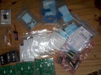
I have a kit available with a board factory populated (JLCPCB) and some additional parts sourced at DigiKey :
- Panasonic FC ecap : 2* 2200uF/50V
- Elna SILMIC ecap : 4* 10uF/50V
- TDK/EPCOS film cap : 4 * 680nF / 1k
- Würth inductor SMD : 1 * 150uH / 770mA / 0.57R
PM me if interested.
Chris
Attachments
Hello,
Nice to see new people interested in the project. Two boards here, available to complement the one from AIM65 and have the 3 needed boards.
Let me know if interested.
JMF
Nice to see new people interested in the project. Two boards here, available to complement the one from AIM65 and have the 3 needed boards.
Let me know if interested.
JMF
Hello,
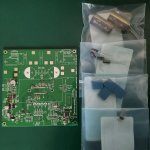
the 3 cards are here and components too, missing the TAS3251 and C8 arriving for the end of June!!!!
I started welding some components and I study the datasheet and note. I can't weld all components because I need place to weld the TAS. I'm going to weld some connectors and test supply voltage and wait.
I have customized the heatsink too.
To be continued.....
Attachments

- Home
- Amplifiers
- Class D
- [design log] Neat 2x170W I2S in, I2C controlled, integrated DSP amp (TAS3251)