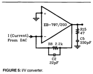
https://www.diyaudio.com/community/...st-tht-i2s-input-nos-r-2r.354078/post-7578753Give us a schematic please. I/V has to exist somewhere (active or passive I/V), the DAC chip is with Iout. I don't remember exactly what I told you. 🤔
Attachments


reduce the supply voltage for the XMOS part to 4V. Then a smaller cooler is sufficient.
The power supply voltage for the XMOS part would be provided by the linear power supply also from JLS- LT 3045 and it is already set to 4V.
Please explain how I can do that with my JLsounds v3, I have the normal version without the extra isolation...
I have both versions of V3. I cut that jumper at the bottom of the PCB and connected the power supply for XMOS where it says in the manual. Since I have a fixed +5V regulator (LM1117T-5.0), I put a 1N4001 diode in the plus line from the regulator to JLS. The voltage drop across the diode at that current (slightly less than 400mA) is about 900mV. A 2.2-2.5ohm 2W resistor can be placed instead of a diode. This reduced the dissipation on the BD139 by 0.3-0.4W. The power supply for the XMOS has a separate secondary 8-9VAC so that it is galvanically isolated from the rest. I grounded supply GND via 100nF + diode bridge 10A to the IEC connector GND (or to the grounded chassis for metal boxes).
Last edited:
I've got devices that are 10+ years, no issues whatsoever. So shouldn't be an issue here. You can always fix usb port from jlsounds to chassis via rubber. It will add to rigidity.But how long does it take until the USB connector breaks from the small PCB
I remember now. That immediately seemed to me like a better option. I hope it can't affect the Iout badly when switching on and off. Connect the instrument to the output of that circuit and monitor the voltage during transients, on&off. Let's say a classic OPA when it is turned on quickly reaches around 0V at the output (with a small DC offset of a few mV), but when the power is turned off and the supply voltage drops below the minimum for the operation of the OPA (say below +- 3V), a DC voltage of the order of 2V appears at the output. And the output of the OPA is connected to the Iout leg of the DAC chip via an I/V resistor. So far, I haven't lost a single DAC chip because of that OPA behavior, but the question is what would happen in case of higher voltages at the output?
Last edited:
I have both versions of V3. I cut that jumper at the bottom of the PCB and connected the power supply for XMOS where it says in the manual. Since I have a fixed +5V regulator (LM1117T-5.0), I put a 1N4001 diode in the plus line from the regulator to JLS. The voltage drop across the diode at that current (slightly less than 400mA) is about 900mV. A 2.2-2.5ohm 2W resistor can be placed instead of a diode. This reduced the dissipation on the BD139 by 0.3-0.4W. The power supply for the XMOS has a separate secondary 8-9VAC so that it is galvanically isolated from the rest. I grounded supply GND via 100nF + diode bridge 10A to the IEC connector GND (or to the grounded chassis for metal boxes).
Thanks! I power the JLsounds v3 from the USB and use only one extra PSU for the clean side. So that means I would need to drop the voltage coming from the USB to around 4V? Since USB has varying voltages I would need to use an LDO to get the 4V, or is it safe to just insert a diode in the VUSB line before the JLsound board?
So you don't want to make a separate power supply but use +5V from the USB port?
For lowering the voltage to +4V, the LDO is certainly a best option. And a standard Si diode (or resistor) will also work, I don't expect any problems there. You can also make a RC filter there, for noise suppression.
A separate +4V internal power supply is probably the best thing.
For lowering the voltage to +4V, the LDO is certainly a best option. And a standard Si diode (or resistor) will also work, I don't expect any problems there. You can also make a RC filter there, for noise suppression.
A separate +4V internal power supply is probably the best thing.
You might have already known but i just want to say that you do not need the shifter ICs on the DAC board if you are using the JLSounds board.My work in progress so far ... I started with a normal USB-powered I2S board configuration, but then I decided to use a separate PSU. Due to some limitations, It would not be possible to use a normal Modushop stainless steel base plate, I will have to find another way. I am still waiting for Burson audio OPAMP. Hope I will finish it next week.
Yes, many users in this thread reported better sound signatures when they were using JLSounds board and skipped the shifters. Anyway, I did not tried this configuration. Maybe I should. Have you personally been able to hear the difference?
And a standard Si diode (or resistor) will also work, I don't expect any problems there. You can also make a RC filter there, for noise suppression.
Ok, I will try. I already tried to use a dedicated regulator from my existing PSU for the USB part, but that sounded worse, probably because GND was shared with the other regulators. A separate PSU should solve this, but for now I will power it from VUSB.
So I guess I can use the jumper at the underside of the JLsounds board to wire in a diode or RC filter...?
ADP7142 or ADP7182 are excellent regulators for these purposes. ADM7150 is much better, but it is also worse than Walt's shunt.These are the external psu’s for the JLS board for my DAC.
The higher current USB section is fed 4V7
I was annoyed by the too strong light from the LCD display, so instead of the current limiting SMD resistor of 100 ohms (R8 on the PCB) I put a serial connection of 100 ohm resistor and a trimmer in front of the LED. The ideal trimmer value is 500 ohms. I didn't have that one, but I put a 2k2 trimmer and a 680 ohm resistor in parallel. It is not linear but it can be adjusted. That's why you should take a 500ohm trimmer to make a nice and smooth lighting adjustment. It is a 1602 LCD display that comes with the AK4113/4118 SPDIF receiver card. Or bought separately, it doesn't matter, they are all the same. Yellow/green is in kit by default. You can buy separately other colors, blue one is the best.
Attachments
Last edited:
I have just changed one of Miro Dacs using JLS and bypassing the shift registers, very noticeable improvement in SQ.Yes, many users in this thread reported better sound signatures when they were using JLSounds board and skipped the shifters. Anyway, I did not tried this configuration. Maybe I should. Have you personally been able to hear the difference?
It should be like that. That jumper is on the +5V power supply from the USB port. It was only necessary that the voltage does not drop below 4V in order for the voltage regulators on the PCB to work properly.So I guess I can use the jumper at the underside of the JLsounds board to wire in a diode or RC filter...?
I sincerely don't recommend using i²s with lengths over 15cm.. the shorter the better. Just because it can, doesn't mean it should.
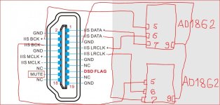
Length is not a problem. Usually such I2S cables are very short. I'm interested if above schematic is correct.
- Home
- Source & Line
- Digital Line Level
- DAC AD1862: Almost THT, I2S input, NOS, R-2R