
Or a scam site designed for DIYers. 🤣Too good to be true? Or did they accidentally buy an old warehouse, and there is everything we need inside, forgotten on the shelves? 🤣
No AD1865 is also segmented dac structure. It is from datasheets. Someone alsi posted internal structure diagram...And what about AD1865 and PCM63, what is their internal structure?
AD1865 is mentioned everywhere as a pure R2R DAC. That's why it was first on my list, except that it's easy to get and not too expensive.
PCM63 probably the same (but with 2 internal dacs in co-linear mode).
I had some internal structure modules i will try to find and post.
By digging a little on that site you may find a TDA1862 triple crown and with a little luck if the month's employee is managing your shipment you could receice a BMW320D ... oups D was not for Dac. ...firered!What do you think about PCM63P-K2 made in Hong Kong?
https://www.ic-components.com/products/PCM63P-K2.jsp
Is this site real ?
Nope...PCM63 probably the same (but with 2 internal dacs in co-linear mode).
Colinear architecture use bipolar zero with small steps in
both directions. Any number of bits can precede the 20 bits to be loaded
I put a link in my post for the published version, but it already has upgrades that have not been published yet.The Jung Shunt Regulator has already been published and is public property.
It is not wide band and gets inductive at HF. It only has low noise and lots of gain at LF.
There are better wide-band regulators around.
My 2 cents,
Patrick
I've compared it to the ADM7150 and a lot of other regulators (serial and shunt) in my DAC and Walt's shunt beats them all in the HF area and noise ( visible on the scope) . I also use it as a regulator for the PMD100 filter.
Igor
What is happening when these regs are far from the load VS another more little IC reg less good in but ultimatly nearer or close from the load ? Impedance, inductive long traces... long current loops...
Which one is winning when it comes to the listening test ?
Which one is winning when it comes to the listening test ?
All good, I got in contact with them and could resolve the PayPal mess…Does anyone has a contact at JLSounds for me. I ordered their I2SoverUSB yesterday, or better said I tried…
PayPal crashed and didn’t send me back to jlsound homepage. The order is in, at least the money was send BUT PayPal sent a total wrong address! So I spent 112€ on something which will never reach me. Paypal declined my case of cancellation, for whatever reason. I am desperately trying to contact JLSound but didn’t get any response on my email. I didn’t got an order confirmation either. Just the money is gone. PLEASE HELP!
Honestly, I don't know. I always make sure that the distance from the regulator to the load is as small as possible, regardless of whether it is ADM7150 or Walt's shunt. For shunt I usually make small PCBs that are easy to place up to the load itself. For my new DAC with TDA1547 on the main PCB there will be six Walt shunts right next to the load.What is happening when these regs are far from the load VS another more little IC reg less good in but ultimatly nearer or close from the load ? Impedance, inductive long traces... long current loops...
Which one is winning when it comes to the listening test ?
All this is excellently explained in the book ANALOG-DIGITAL CONVERSION by Walt Kester and one of the contributors to the book was Walter Jung.
Attachments
... I like more subjectivly (listening) the ADM7150 and TSA7xx regs than the often seen LT3042. Always wanted to try a pcb with embeded ADM for the 5V rails. I use TSA7 for IanCanada clocks...works better to my ears despite the noise floor of both is very low...maybe an impedance level thing. I found that LiFePo cell no to be better when a reg was needed beforz the clock.
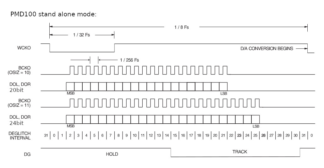
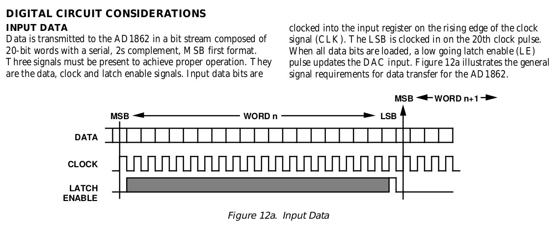
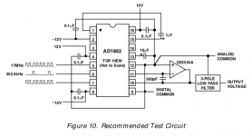
Take a look at the simplified input format of AD1862. That is more like time simultaneous format without inverted MSB, and sign.@miro1360, looking a bit closer at your diagram I think it might not work that way. From the PCM1702/4 datasheets: "if BCLK is stopped between input data words, the last 20/24 bits shifted in are not actually transferred from the serial register to the parallel DAC register until WCLK goes LOW. WCLK must remain LOW until after the first BCLK cycle of the next data word to insure proper DAC operation." This is also shown in the PMD100 datasheet, see this screen shot:
An inverted DG also might work as WCKO. Here is what I think how your digram could look like:
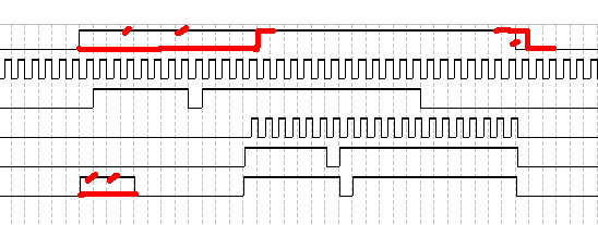
The timing diagram of the AD1862 shows the same requirement: WCKO stays low until after first BCK cycle of DATA transfer, goes high, and goes low again only after last BCK cycle of DATA transfer:
What do you think?
So jut one half of BCK pulse needed to tell the dac to go into DA konversion... On the figure 12a all of unnecessary Hi states are marked GREY.
BUT that is the "minimal" margin to the RIGHT border.
Now, take a look at the PMD100 output format.
It is NOT shifted at the very end of possible word-to-LE.
But opposite - there is a "room" of plenty of BCK cycles even for the 24bit word.
So the dac after receiving all serial bits conducted with BCK, have some time to "rest" and "settle down".
DAC dont rush into conversion immediately, like almost instantly when LSB loaded. It is close to impossible...
That is why Pacific Microsonics did different from all other digital filter ICs...
BTW never writen that has to be Righr justified format.
(off-course for 32bit word length it should be packed tightly into 32bit max length
Another thing is that MSB shifted only 1 BCK from I2S standard.
That is totally 2 BCK cycles from last LE of previous converted word.
.
Common thing about WCKO (LE) for almost all Digital filter ICs is that LE divided into 1/4 to 3/4 of total Fs time.
But again DAC does not need that.
Attachments
Hi MiroThe "unwanted" DATA is not feeded into the DAC because the clock is stopped. Making it total clean adds to the complexity 😀
PCM1702/4 is specific (because of the BCK requirement - the jitter in BCK can affect the sound), but the AD1862 has not this requirement and the output depends only on the low going LATCH (jitter in LATCH - LRCK can affect the sound) - That is why I don't want to modify the LRCK signal because the XMOS processor outputs it very clean 🙂
please take a look in I2S Philips specification PDF.
Note WSP and WSD signals. They are essential for managing almost any digital bus.
In PDF given only WSP signal graphically. emulate WSD.
That can be of use to create WCKO (LE), and other events.
The circuits are not complicated to achieve.
.
For these dacs I would not insist on pure Right Justified (like PCM1794 dictate as must) because these earler dacs are not specified as Right Justified.
Maybe try to stick with Pacific Microsonics approach but in NOS mode?
Maybe it is easy to sheck with recent shifter. Just not shift so deep but only 1 bit from I2S MSB all words for L/R?
.
We actualy dont know are the outputs of the XMOS are clean? Maybe just for the scope eye pattern on the scope? (But even then looking like have bigger peaks at the corners of the squares - signal integrity)
But from the point of jitter and eye pattern in time we don't, and that is the only criteria for clean?
.
BTW
From my measurements most of the XMOS based interfaces has inverted MCK. (That is not happier for re-clocking and other purposes of MCK.
Amanero have right edged MCK for the example.
Attachments
Last edited:
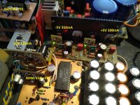
Sounds interesting. As long as there's not too much smd work this could be fantasticWith all the power supply discussions recently, seems like a perfect time to ask opinions about what types of psu would be favored to include onboard an AD1862 dac. After building several versions of MiroDac the common source of “clutter” always seems to be the multiple external power supply boards needed. I’d like to clean up this aspect of the build and leave off-board real estate options for I/V and output stages.
4 supplies would be minimum, +/-12v and +/-5v but possibly 6 supplies if onboard I/V (opamps) will be independent from dac chip supply.
In order to make an all inclusive board such as this, space would have to be used carefully thus requiring the use of some SMD components. What do you guys think?
SMD is easy guys as far you still can see the legs of IC/parts you are soldering and have flux, below that size it is indeed another story... still feasible with 0603 packages for enthusiast with magnyfing glasses... while not necessarily needed always but to please the scopes.
Why are you bombarding the topic with digital filters ? I mean you're going in with the digital filter story to ruin the DAC theme that it doesn't have and shouldn't have. We have consciously rejected what should be at the DAC entrance outside the manufacturer's recommendations.That is why Pacific Microsonics did different from all other digital filter ICs...
Last edited:
No AD1865 is also segmented dac structure. It is from datasheets.
Indeed so, here's the relevant part :
We actualy dont know are the outputs of the XMOS are clean?
That's why you have two power supplies on the JLSound I2SoverUSB - which are galvanically separated from the computer USB and its SMPS and any noise that the motherboard can produce. The goal is to have only D + and D- at the XMOS input. But if that's not enough for your purist mind, there are PCI USB cards with high-precision XO oscillators. And you don't need any filter in the world for this.
Last edited:
No?Why are you bombarding the topic with digital filters ? I mean you're going in with the digital filter story to ruin the DAC theme that it doesn't have and shouldn't have. We have consciously rejected what should be at the DAC entrance outside the manufacturer's recommendations.
Maybe it is only yours wrong interpretation 🙁
It is not story about digital filters and OS at all...
.
I just reply once to the post that other member note about input formats.
But not with opposing, just to give the other complementary opinion based on published data?
And i gave some arguments. this is the reply please read again...
.
https://www.diyaudio.com/community/...st-tht-i2s-input-nos-r-2r.354078/post-7053672
.
I just analyzed the format considering NOS mode.
And within the manufacturers AD1862 recommendations illustrated by data from the datasheet?
.
cheers
Please understand that there is no galvanic isolation from the computer in case of just separate power supply to the USB interface. This is not true because +D and -D have to refer to the GND plane that is common even with external PS. Noise from motherboard transferring via ground plane into the USB interface too...That's why you have two power supplies on the JLSound I2SoverUSB - which are galvanically separated from the computer USB and its SMPS and any noise that the motherboard can produce. The goal is to have only D + and D- at the XMOS input. But if that's not enough for your purist mind, there are PCI USB cards with high-precision XO oscillators. And you don't need any filter in the world for this.
.
Please try to recognize 3 types of "clean"
1. clean power supply - helps, members experimented lot and posted results
2. clean oscilloscope shape pattern - that is already presented in form of by different measurements that members did. And the signals in these termas are not so clean but with glitches and ground bounces.
3. clean eye pattern in period of time - related to jitter and longer time domain that is important. Special equipment...
.
Please don't tend to be hostile?
- Home
- Source & Line
- Digital Line Level
- DAC AD1862: Almost THT, I2S input, NOS, R-2R