
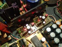
Thank you for this internal structure, very interesting 🤩Some AD1862 porn I came across recently, needs sharing where there's a hotbed of 1862 worship😊
View attachment 1065306
No impact for AD1862 or AD1865 as long as the LRCK is not touched 🙂 ... but this is not true for PCM1702, PCM1704, PCM63 and other DACs where the output is updated on the BCK cycle.So shift register or FGPA choice do have no impact here for the bclk channel and final sounding quality ?
I will CNC that below 🤣Delta Sigma Destroyer 🥷
I have to agree with Zoran with the use of shunt regulators in DAC, they are much better options than serial regulators. I started installing the first shunt regulators in my DACs about 10 years ago and was surprised by the improvement. Now I am using an improved version of the shunt regulator from Mr. Walt Jung, the picture shows a +/- 5V shunt for my PCM1702 (6 pcs.), The current is 250mA for - and 100mA for +.Yes I tried shunts at the DAC PS and they are very good. BUT as close to the DAC chip and for each power pin. In that case grounds are close to each other and dissipation from power "loss" is not huge, no overheat because it spread to more little shunts. Main power could be central Vd and Va.
in that case 4 shunt regs modules needed for each dac chip and it should be integral part of DAC pcb close to the power pins and ground planes.
.
It make an overall sound improvement when aplied in all digital modules like separate shunt gor the re-cklocking, digiral isolation and so. Same way close to the modules.
.
For shunt is some advice to have 120% of current that source is consume. So for the 100mA we need another 120mA that is 220mA for unloaded shunt. That should be NOT overheated without load! For stabler operation and proper testing witout load bare in mind bigger hat-sinks for larger current loads 🙂
.
Anyway my experience is very good.
This improved version was done together with Mr. Walt and I hope that the circuit will be available to everyone soon. Unfortunately, these regulators are not simple and have a slightly higher dissipation than the serial ones, but they are worth the effort.
Attachments
Does anyone has a contact at JLSounds for me. I ordered their I2SoverUSB yesterday, or better said I tried…
PayPal crashed and didn’t send me back to jlsound homepage. The order is in, at least the money was send BUT PayPal sent a total wrong address! So I spent 112€ on something which will never reach me. Paypal declined my case of cancellation, for whatever reason. I am desperately trying to contact JLSound but didn’t get any response on my email. I didn’t got an order confirmation either. Just the money is gone. PLEASE HELP!
PayPal crashed and didn’t send me back to jlsound homepage. The order is in, at least the money was send BUT PayPal sent a total wrong address! So I spent 112€ on something which will never reach me. Paypal declined my case of cancellation, for whatever reason. I am desperately trying to contact JLSound but didn’t get any response on my email. I didn’t got an order confirmation either. Just the money is gone. PLEASE HELP!
With all the power supply discussions recently, seems like a perfect time to ask opinions about what types of psu would be favored to include onboard an AD1862 dac. After building several versions of MiroDac the common source of “clutter” always seems to be the multiple external power supply boards needed. I’d like to clean up this aspect of the build and leave off-board real estate options for I/V and output stages.
4 supplies would be minimum, +/-12v and +/-5v but possibly 6 supplies if onboard I/V (opamps) will be independent from dac chip supply.
In order to make an all inclusive board such as this, space would have to be used carefully thus requiring the use of some SMD components. What do you guys think?
4 supplies would be minimum, +/-12v and +/-5v but possibly 6 supplies if onboard I/V (opamps) will be independent from dac chip supply.
In order to make an all inclusive board such as this, space would have to be used carefully thus requiring the use of some SMD components. What do you guys think?
Last edited:
The Jung Shunt Regulator has already been published and is public property.
It is not wide band and gets inductive at HF. It only has low noise and lots of gain at LF.
There are better wide-band regulators around.
My 2 cents,
Patrick
It is not wide band and gets inductive at HF. It only has low noise and lots of gain at LF.
There are better wide-band regulators around.
My 2 cents,
Patrick
With all the power supply discussions recently, seems like a perfect time to ask opinions about what types of psu would be favored to include onboard an AD1862 dac. After building several versions of MiroDac the common source of “clutter” always seems to be the multiple external power supply boards needed. I’d like to clean up this aspect of the build and leave off-board real estate options for I/V and output stages.
4 supplies would be minimum, +/-12v and +/-5v but possibly 6 supplies if onboard I/V (opamps) will be independent from dac chip supply.
In order to make an all inclusive board such as this, space would have to be used carefully thus requiring the use of some SMD components. What do you guys think?
You can't avoid a lot of DC power supplies with devices like this. I made DDDAC1794, 4 boards, I counted almost 20 voltage regulators.
Last edited:
I have bought and received a total of 3 so far. Each time I contacted JLS to send me a Paypall link. Since Bulgaria is in the neighborhood, I paid postage much less than you (ordinary post with tracking). In total, it was around 77 euros. I hope that in contact with JLS you can solve that.Does anyone has a contact at JLSounds for me. I ordered their I2SoverUSB yesterday, or better said I tried…
PayPal crashed and didn’t send me back to jlsound homepage. The order is in, at least the money was send BUT PayPal sent a total wrong address! So I spent 112€ on something which will never reach me. Paypal declined my case of cancellation, for whatever reason. I am desperately trying to contact JLSound but didn’t get any response on my email. I didn’t got an order confirmation either. Just the money is gone. PLEASE HELP!
Hi MiroDigital Filter YSF210B-D (8x oversampling)
Here is a shot schematic for digital filter YSF210B-D.
I am almost sure it will gain zero interest, therefore no PCB.
I have ever read on the internet that it is close to the PMD-100 filter (maybe not so good, but better than the DF1704 waster).
It supports the same sampling frequencies as the PMD-100 (only up to 48kHz).
I share the schematic - what if someone in the future will decide to test it on a breadboard for the good of the soul? 😀
(asynchronous mode should be selected with 21.168MHz clock)
there are some digital filters that could be replacement for Pacific Microsonics obsolete IC PMD100 (only capabile for stand alone operation)
https://manualzz.com/doc/30053242/hdcd-ics-for-consumer-audio
BTW You should use Master clock divider by 2 from USB/I2S for input at the DF that can a;ready done in other topic PMD100 to TDA1541A TS mode.
HiFor your reference, I found this graph that I believe was originally posted by diyinhk on some audio forum a few years ago:
View attachment 999633
Yes BUT this is mainly from issues with signal integrity and ground bounce-s.
Related to the phenomenon that signal can go higher than V+ and lower than ground 0V.
.
AND interfering different F in the extremely small distances in the ICs.
.
The cure is FIRST to solve signal integrity between each IC with the simple R.
And for the ground bounces careful decoupling and maybe shunt as close to the modules doing the same thing.
.
Digital ICs are designed to drive as up to 16 other digital IC inputs. So they are solid drivers. But in most of the aplications they not driving more than few. So the driver is much sufficient then needed. With small capacitance of the next stages to drive. Solution is to add more R at the output and trimm the peaks at the edges of the square signal. That is for signal integrity for ground bounce is different but could be decreased with aplied sig .int.
.
Stopped clock is next thing to do.
.
Ground bounce, Signal integrity
Last edited:
JLS is a modern high-tech device. Not a blast from the past at all.But it emulates these old chips.The only complaint for me is that it is too small.I have bought and received a total of 3 so far. Each time I contacted JLS to send me a Paypall link. Since Bulgaria is in the neighborhood, I paid postage much less than you (ordinary post with tracking). In total, it was around 77 euros. I hope that in contact with JLS you can solve that.

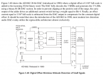
Actually that is explanation that AD1862 is NOT pure R2R dac.Thank you for this internal structure, very interesting 🤩
But segmented DAC or hybrid DAC.
Because first 3 bits are transformed as 7 bits of Thermometer code. And going to conversion same as DSD.
Other low significant bits are classic R2R dac...
So most of the sound comes grom generated first 7 bits 🙁
As other AD and PCM dacs...
Attachments
And what about AD1865 and PCM63, what is their internal structure?
AD1865 is mentioned everywhere as a pure R2R DAC. That's why it was first on my list, except that it's easy to get and not too expensive.
AD1865 is mentioned everywhere as a pure R2R DAC. That's why it was first on my list, except that it's easy to get and not too expensive.
Last edited:
And that it needs two separate + 5V power supplies for maximum effect (galvanic isolation).The only complaint for me is that it is too small.
Last edited:
What do you think about PCM63P-K2 made in Hong Kong?except that it's easy to get and not too expensive.
https://www.ic-components.com/products/PCM63P-K2.jsp
Is this site real ?
Last edited:
- Home
- Source & Line
- Digital Line Level
- DAC AD1862: Almost THT, I2S input, NOS, R-2R