off-topic: Looks nice! Would you recommend your CNC service?
Desirable Sigma Delta ?
Delta Sigma Dac ?
Droll Sexy Dragon ?
Doing Sarmat Danger ?
Dalaïlama Super Dance ?
Delta Sigma Dac ?
Droll Sexy Dragon ?
Doing Sarmat Danger ?
Dalaïlama Super Dance ?

Anybody has two AD1862 left over. Shipping to Canada, PayPal money transfer. PM me…
DigiKey wants me to buy 14 and Rochester 11, no affordable offer at eBay in the moment…
I am also looking for two op amps OPA627 or NE5534, LM6171 or ADA4989-1 I am not picky on this one.
DigiKey wants me to buy 14 and Rochester 11, no affordable offer at eBay in the moment…
I am also looking for two op amps OPA627 or NE5534, LM6171 or ADA4989-1 I am not picky on this one.
Paddy Garcia in USA has genuine ones https://www.diyaudio.com/community/...st-tht-i2s-input-nos-r-2r.354078/post-7030137
Guys, I was said today with one person - he also know Dac 1862 and he told me about some improvements.
What do you think about these improvements?
Unfortunately I can't get these lv164a (except ali).
- change shift registers on lv164a
- change their feeding to 3,3V with stabs LP5907 or TPS7A2033
- install the others opamps or made a custom output.
What do you think about these improvements?
Unfortunately I can't get these lv164a (except ali).
These regs are smd not through hole...you want our Miro to have an heart stroke or what ?
Deep down, Miro does like SMD 😉….
Most of the forum does not. But the parts situation is rapidly changing how designers will pick parts. So, DIY’ers are going to have to address their hesitation towards SMD soldering in order to keep on slingin’ solder
Most of the forum does not. But the parts situation is rapidly changing how designers will pick parts. So, DIY’ers are going to have to address their hesitation towards SMD soldering in order to keep on slingin’ solder
If you want something similiar to the 74LV164A without changing voltage to the 3.3V (and without changing PCB), use the 74AHCT164D - it has similar speed to the 74LV164A. Changing the PCB for 74LV164A has zero benefit because output of this DAC is based on the LRCK (and LRCK is not affected by shift registers - it goes directly from an I2S device to the DAC) ... so easily get with the 74AHCT164D and you will have the same "benefit" like with the 74LV164A 😉Guys, I was said today with one person - he also know Dac 1862 and he told me about some improvements.
Also he offer to made a digital filter (optional).
- change shift registers on lv164a
- change their feeding to 3,3V with stabs LP5907 or TPS7A2033
- install the others opamps or made a custom output.
What do you think about these improvements?
Unfortunately I can't get these lv164a (except ali).
You can install and test any opamps, as well as a custom output.
Digital filter is very very tricky. Something like PMD200 (or PMD100) can be good, but is really? - hard to obtain and test, ... but something available like DF1704 is very bad 🤢
So shift register or FGPA choice do have no impact here for the bclk channel and final sounding quality ?
Some AD1862 porn I came across recently, needs sharing where there's a hotbed of 1862 worship😊

No, not smd. Here - just like Nexperia soic14 5PCS X 74LV164A, SO14 | eBayThese regs are smd not through hole...you want our Miro to have an heart stroke or what ?
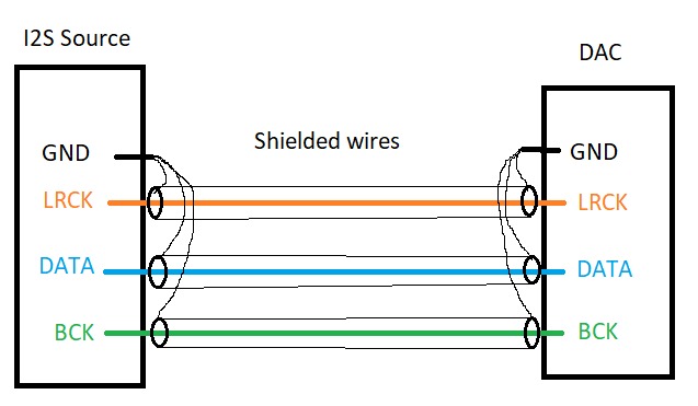
This is not good way of connectio. Try first connect grounds of 2 modules. Even if they powered from the same PS. Then connct the sheilds to ground at the transmitter (driver) side - I2S source. At the dac PCB shields should left un-connected. If the R for the signal integrity needed, apply it closer to the dac input.@Robin De Wolf
24b/192kHz audio should work with this DAC (from that 20 most significant bits will be played). You can test it with an xmos based USB-I2S.
... the DAC logic does support a 64-bit frame I2S ... it does not support shorter bit frames (48 (2x24), 32 (2x16)) ... this 64-bit frame will transfer all stereo music files in resolutions 16-bit, 24-bit and 32-bit (from that 20-bit will be played)
... the question is: Does the RPI support 64-bit frame on 192kHz? RPi 4 should support it, but the older ones may be limited.
... I googled, that RPi 3 does support 24b/192kHz as the maximum, and here I don't know if it sends these bits in a 48-bit frame or can handle the 64-bit frame. If 16b/192kHz is played on the DAC, they are sent in the 64-bit frame, the same for 24/96khz (because it worked), but what is the frame for 24b/192kHz? (I found, that HDMI works only in 16b/192kHz) ...
Try to shorten the I2S wires. Or use a shielded wire for the I2S (but it probably won't be the solution 😕)
Attachments
If you put a digital filter and upsampling in front of the DAC chip, and the only one that doesn't sound very bad is the PMD200, in my opinion you won't get better sound. You will only get better measurements.
For SS3601 one part of the elements around must be soldered from below. Otherwise you will have to nail one or two DIP8 sockets due to the dimensions of SS3601. This OPA sounds really great, I recently have an SS3602 in the preamp. I don't know how they achieved that, and I don't care.
The other part of the story is the JLS I2SoverUSB board. It brings these DACs to a high level. The condition for the best result is that it has a separate power supply 5VDC 400mA for the input part with XMOS chip (this must be galvanically separated from the rest, with separete secondary 9VAC), and separate 5VDC 100mA for the output part with oscillators. And to cut the jumper from below on the JLS which separates the USB power supply + 5V.
Yes I tried shunts at the DAC PS and they are very good. BUT as close to the DAC chip and for each power pin. In that case grounds are close to each other and dissipation from power "loss" is not huge, no overheat because it spread to more little shunts. Main power could be central Vd and Va.Shunt regulators
Did someone listening test between any series voltage regulator and a voltage shunt regulator? (on any R-2R DAC).
There are plenty modifications of Salas shunt regulator. Since it's a shunt, I wouldn't want any active element in the series, so I slightly simplified one from 2009 and put 2 in a row. It holds the voltage under any load. The mirror version for the negative will be similar.
The main drawback of shunt regulator is the large power losses, in my case 20W 😡
No real test was performed by me, maybe it's not even stable.
Whether it makes sense to try ...
in that case 4 shunt regs modules needed for each dac chip and it should be integral part of DAC pcb close to the power pins and ground planes.
.
It make an overall sound improvement when aplied in all digital modules like separate shunt gor the re-cklocking, digiral isolation and so. Same way close to the modules.
.
For shunt is some advice to have 120% of current that source is consume. So for the 100mA we need another 120mA that is 220mA for unloaded shunt. That should be NOT overheated without load! For stabler operation and proper testing witout load bare in mind bigger hat-sinks for larger current loads 🙂
.
Anyway my experience is very good.
- Home
- Source & Line
- Digital Line Level
- DAC AD1862: Almost THT, I2S input, NOS, R-2R