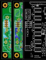
v2.0 AD1862 NOS Stop-Clock
Here is the Stop-Clock version
Be careful - it is something new and design is untested, so it may not work
Analog-Digital ground layout has been added (merged under DACs) 🙂
Here is the Stop-Clock version
Be careful - it is something new and design is untested, so it may not work
Analog-Digital ground layout has been added (merged under DACs) 🙂
Attachments
-
diyAudio_AD1862_DAC_v2.0_Stop-Clock_2021-11-25.zip651.7 KB · Views: 131
-
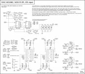 diyAudio_AD1862_DAC_v2.0_Stop-Clock_Schematic.jpg765.5 KB · Views: 561
 -
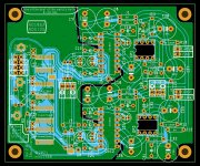 diyAudio_AD1862_DAC_v2.0_Stop-Clock_pcb.jpg783.6 KB · Views: 552
 -
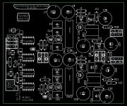 diyAudio_AD1862_DAC_v2.0_Stop-Clock_parts.jpg318.2 KB · Views: 433
 -
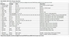 diyAudio_AD1862_DAC_v2.0_Stop-Clock_BOM.jpg380.5 KB · Views: 484
I saw this, but it would make more sense if both channels were stopped - and he claims that to be the case as well. Did you check the Naim circuit for stopped clock?
Not yet. Can you post the schematic? What do you think about?
For schematics of the Naim see this post.
The stopped clock circuit is in the PDF named "R4" which you will find in the folder "main": look at the circuit right of the PMD200 on page 2 of the PDF. I posted a screenshot of it here.
The timing of the stopped clock is described in the data sheets of PMD100 and PCM1704.
The stopped clock circuit is in the PDF named "R4" which you will find in the folder "main": look at the circuit right of the PMD200 on page 2 of the PDF. I posted a screenshot of it here.
The timing of the stopped clock is described in the data sheets of PMD100 and PCM1704.
Last edited:
Yes, I know. It's a CD-player, and a very good sounding one. But my point was about the stopped clock circuit 😎
Off topic question: I'm having trouble finding the right pin connectors for the Jl sounds i2s board to Miro board
Hidy and Miro, can you share part numbers for how you connected the i2s board? Hidy maybe some close up photos?
Hidy and Miro, can you share part numbers for how you connected the i2s board? Hidy maybe some close up photos?
@jpk73 The clock is not stopped for PCM1704 DACs 🙂
Miro, what do you mean...? The Naim uses stopped clock for PCM1704, and the datasheet of PCM1704 has a section about stopped clock operation!
Am I missing something...? 😕
@jpk73 See the main board diagram on the first page (CDS3main_R4.pdf)
There is only one CLK common for both DACs, therefore it cannot be stopped.
There is only one CLK common for both DACs, therefore it cannot be stopped.
Off topic question: I'm having trouble finding the right pin connectors for the Jl sounds i2s board to Miro board
Hidy and Miro, can you share part numbers for how you connected the i2s board? Hidy maybe some close up photos?
I am using diyinhk xmos dac board stacked right on top of miro's dac inputs. The pins are compatible.

Here is the Stop-Clock version
Be careful - it is something new and design is untested, so it may not work
Analog-Digital ground layout has been added (merged under DACs) 🙂
Thank you miro! This is so exciting! I would like to build a stopped clock version as my my next project. Meanwhile, If anyone has got spare pcbs to share for this version, please pm me. Thanks.
Today, after some tweaking, I've got my THD measurement down to 0.00288%. This is better than my diyinhk dac's performance. The sound is a joy to hear. AD1862's max performance is around 0.002%. I think I have gone as far as I can go with the 1.3 version and will happily stop tweakingng my dac and start enjoy some music now.
Cheers!
Here is the Stop-Clock version
Be careful - it is something new and design is untested, so it may not work
Analog-Digital ground layout has been added (merged under DACs) 🙂
Hi miro,
What is the dimension of the version 2.0 pcb? Is it the same size as version 1.3?
Are the positions of the pins 1 to 6 of the I2S inputs exactly the same as those in version 1.3? I am asking this because I have already drilled a usb hole in my dac case. I will need those pins to be in the same exact positions to be able to continue to use the same hole.
Do you think 2OZ copper thickness will sound better than 1OZ?
Thank you.
Hidy
Last edited:
@asilker
You can order it from ebay 2.54mm Pitch Single/Double Row Female Header Socket Connector For PCB 2 to 40Pin | eBay
(double row 20 pin, and single row 10 pin) 🙂 ... @meanie built this version
You can order it from ebay 2.54mm Pitch Single/Double Row Female Header Socket Connector For PCB 2 to 40Pin | eBay
(double row 20 pin, and single row 10 pin) 🙂 ... @meanie built this version
@Hidy
What is your tweaking for such good THD? 🙂
The stop-clock version is untested. Prepare yourself for headache 😀
Dimmensions and pins are the same (you can use 2x3 pin header).
I doubt 2oz DAC will sound better than 1oz 🙂 ... but power amplifier can sound better.
What is your tweaking for such good THD? 🙂
The stop-clock version is untested. Prepare yourself for headache 😀
Dimmensions and pins are the same (you can use 2x3 pin header).
I doubt 2oz DAC will sound better than 1oz 🙂 ... but power amplifier can sound better.
Attachments
@Hidy
What is your tweaking for such good THD? 🙂
I did these things:
1) Added 2 x 270uf 16v Oscon capacitors to bypass +-12V power input on board. I feel that they are important for improving channel cross talk performance by canceling/damping the what I call crossfire effect where the currents/signals from the 8 x 100 uf caps are influencing each other through this intersection;
2) Replaced all 8 x 100 uf Elna Silmic with 8 x 270uf Oscon solid capacitors. This removed the Elna sound signature as well, but more importantly, the voltages at power pins became even more rocket solid. My oscilloscope showed a beautiful flat line with a thickness of 20mv with Oscons.
3) Followed the AD1862 data sheet strictly.
I changed the feedback resistor from 1k5 to 3k, simply because I feel AD1862 might be optimized for a 3k value by design. AD1862 has its own laser-trimmed 3k feedback resistor on the chip. And its data sheet also recommended 3k as well. I tried both 1k5 and 3k and I like the 3k sound better even though my 1k5 resistors had superior specs with tolerances of 0.02% and extremely low ppm. These resistors are very expensive. But I broke one of them after soldering and desoldering them a few times. My 3k resistors have a tolerance of 1%.
I changed the feedback caps to 82pf plus a 100R resistor. The resistor is important to avoid oscillation.
I also added 2000pf to pins 2 and 3 of AD797, right on the soic to dip8 adapter. I tried putting these on the dip8 socket, but this ruined the channel crosstalks. They dropped from 87 to 53 db. I guess that putting the input shunt resistors too close to the ground plane causes the signals of one channel to leak into the other channel through the cap 1 - ground - cap 2 connections.
One more thing I have learned through all these tests is that the left channel is consistently quieter than right channel. They have different noise patterns. My tweaking did not succeed in affecting the noise patterns at all. The left channel is alway flat across all frequencies. But the right channel is V shaped. It starts with 10 db higher noises at low frequencies, then dropped to below left channel's noise level at medium frequencies, and eventually become slightly more noisy at high frequencies.
Switching left and right dac chips doesn't change the noise patterns either. Changing output lineout cable positions also doesn't work. I believe that the differences are caused by pcb layout as the pcb is not symmetrical.
@miro, this is a major opportunities for improving the pcb layout. I would suggest duplicating your left channel layout for the right channel. This will make the right channel as quiet as the left and improve the dac's overall performance.
If there is a way to link layout to frequency performance, I would say for low and high frequencies, following the left channel layout; for medium frequencies, follow the right channel layout.
What a perfect world this would be if we can pick and take only the best part of pcb layout of each channel. Hahaha🙂🙂🙂
Hidy
maybe dual mono DAC pcbs? I know the power supply scheme is selectable with jumpers but my wish list would include seperate digital and analog power into the board for each channel on opposite sides of the board. (although I am already grateful for what our generous host has published)
4-layer PCB highly recommended, possibly with segmented ground plane areas. Not trying to be a critic of the development work so far, just would like to see folks to end up with a little better dac. Unfortunately, don't have time to commit to board design myself.
Regarding those little organic polymer electrolytic caps, they measure as pretty linear but their noise behavior is not something I would want on an analog circuitry rail. IME those caps sound awful in circuits where they can be heard. Probably fine for fully digital circuitry, bearing in mind that things like clocks and or PPLLs, etc., are analog. Suggest to avoid ferrite beads for analog circuits too, if possible.
Regarding those little organic polymer electrolytic caps, they measure as pretty linear but their noise behavior is not something I would want on an analog circuitry rail. IME those caps sound awful in circuits where they can be heard. Probably fine for fully digital circuitry, bearing in mind that things like clocks and or PPLLs, etc., are analog. Suggest to avoid ferrite beads for analog circuits too, if possible.
Last edited:
@Hidy Thank you for all your hints 🙂
The stop-clock PCB contains gaps in the GND plane, between digital and analog, and GNDs are connected under DAC chips ... it can improve something, or maybe not, hard to say without testing 🙂
I still think these LDO regulators have big problem with capacitors. Can you test the 78/79xx regulators how they perform in comparison with the LDOs? 😀
- Home
- Source & Line
- Digital Line Level
- DAC AD1862: Almost THT, I2S input, NOS, R-2R