A ccs loaded triode is one way of doing it, but if you can design tube circuits there are other options you might prefer. There are always choices in DIY - choices of op-amps, choices of tubes.
But I guess most will want to keep it simple in this particular application and follow the usual schematic. Which is fine.
But I guess most will want to keep it simple in this particular application and follow the usual schematic. Which is fine.
Last edited:

Pardon the mess, just testing if the programming on the CPLD is successful. I just want to say that Miro's 24Bit VHDL programming works perfectly. Converts i2s to PCM using a CPLD board, skipping shift registers ( are they really that bad?) , and using an existing Amanero USB interface. Building this for a friend who does not want to invest in a new USB interface ( York, JLsounds) .
Works perfectly, no noise no digital glitches. On the actual implementation, the wires will be very much shorter, of course it has to be.
Works perfectly, no noise no digital glitches. On the actual implementation, the wires will be very much shorter, of course it has to be.
Attachments
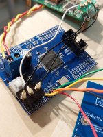
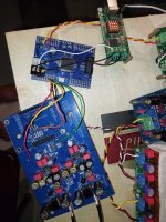
Ok, i have adapted the CPLD board to be stacked on the DAC board just like the JLSounds I2SoverUSB FIO (http://jlsounds.com/i2soverusbFIO.html) and York with reclocker (https://www.diyaudio.com/community/...tichannel-input-output-interface-york.413504/).
Now i can use any USB-I2S interface via the u.fl connectors i have installed on the CPLD board.


Now i can use any USB-I2S interface via the u.fl connectors i have installed on the CPLD board.
Ok, some may have known but there were a couple of members who DM me about the CPLD board and free code.
They are all in Miro's blog, post #1.
https://electrodac.blogspot.com/p/dac-ad1862-almost-tht-i2s-input-nos-r.html
Look for these, they are near to the bottom of the blog page :

They are all in Miro's blog, post #1.
https://electrodac.blogspot.com/p/dac-ad1862-almost-tht-i2s-input-nos-r.html
Look for these, they are near to the bottom of the blog page :
https://vi.aliexpress.com/item/1005...t_main.29.611c1802hcSClX&gatewayAdapt=glo2vnm
My friend took these, and it works. There are over 3000 of them in stock, so they will last. 😁
My friend took these, and it works. There are over 3000 of them in stock, so they will last. 😁
Guys, built tda1541 with ad797, and...
What I wrote in private to a fellow...
"is the most colored, far from neutral, emphasized combination I've ever heard!
And I don't know if it's good or bad...
Need to listen to it with headphones, something sounds quite suspicious to me."
Does anyone agree? 😂
What I wrote in private to a fellow...
"is the most colored, far from neutral, emphasized combination I've ever heard!
And I don't know if it's good or bad...
Need to listen to it with headphones, something sounds quite suspicious to me."
Does anyone agree? 😂
I have preferred to respond to you in private 🤣Does anyone agree?
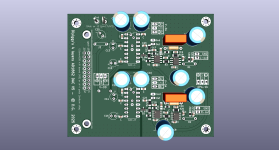
Finished the last V5 iteration of my 4 layers AD1862 pcb and ordered a batch of 5 pcb.
It has the same features of the last : designed for high speed single opamp. Has a voltage follower (buffer, etc) op amp that can be easily bypassed but can be usefull for ome I/V op amps, headphones or digital volume chips.
4 layers to enhance the capacitance of the ref layers and to avoid signals and power crossings with a carefull routing and forced current paths playing with the layers and THT decoupling.
Independant power inputs for the op amps.
Made to work with I2Sover USB v3 board or 4 uf-l pads at the bottom side for iancanada I2StoPCM board or any DIY USB to AD1862 front end.
What I added in the V5 is the possibility to use not only the VFA op amps but also the CFA (it is compatible with AD811 Grünf dissident design but in SMD version of the AD811) and the transconductance OPA861 in emitter input transimpedance mode. That's is for I/V first op amp. The second op amp is only a voltage follower for buffer (G+1) or more gain.
It was a little tricky to find the good layout for the op861 layout pcb compatibility w/o sacrificing quality. But I added via a jumper the possibility of its use with the choice of either SMD or/and through hole Resistor i/V and Capacitor i/v as it is important in my experience to voice it for best results.
It has also an output and Gnd vias near the AD1862s to plug a pcb for a future discrete I/V design or wirering for tubes with or w/o the possibility to proceed of the passive I/V (smd).
Output protection for the AD1862 and filtering options via passive smd caps and/or resitor (Rutgers pdf for illustration) were enhanced and permitts the use of external compensation.
Attachments
Last edited:
Very nicely done! Looking forward to seeing the first builds with that PCB. 🙂 🙂
Have made a pretty BOM at Mouser with 3 new op amps included the AD811 and the expensive resistors Grunf advised for it...
I have made last years sevral 4 layers proto you can see in the thread to use some opamps combo...
I'm looking forward to use the op861 with a Rhopoint resitor and its tin foil polystyrene caps which had given very good result in my main TDA1541A dac. If not giving the same magic, i wanted to add two smd resistor and caps options to have the possibility of a theorical better layout than the throug hole option for the op861 I/V.
- Home
- Source & Line
- Digital Line Level
- DAC AD1862: Almost THT, I2S input, NOS, R-2R