hi miro,
i am doing the pcb with stacked I2SoverUSB III and planning to use tube buffer for IV
if so, C29, C27, C28, C30, C31 and C34, C32, C33, C35, C36 are not needed to install?
Thank in advance
happy
i am doing the pcb with stacked I2SoverUSB III and planning to use tube buffer for IV
if so, C29, C27, C28, C30, C31 and C34, C32, C33, C35, C36 are not needed to install?
Thank in advance
happy
which tube(s) do you intend to use?hi miro,
i am doing the pcb with stacked I2SoverUSB III and planning to use tube buffer for IV
if so, C29, C27, C28, C30, C31 and C34, C32, C33, C35, C36 are not needed to install?
Thank in advance
happy
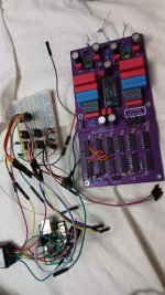
My prototype of the TDA1541A plays quite well, nice clean output 
Time to buy out the whole eBay and rise the price of this DAC even more LOOL 🤣
Time to buy out the whole eBay and rise the price of this DAC even more LOOL 🤣
- no digital filter, NOS
- full THT with glue-logic to maintain the nostalgia
- simultaneous mode (I2S input)
- big foil capacitors
- power supplies will be on the PCB (78/79xx regulators)
- opamps remain for the I/V
Attachments

My prototype of the TDA1541A plays quite well, nice clean output
Amazing. Another great DAC design, that you also found time to build. Nice TDA1541a chip too 🙂
I hope you dont mind me asking the usual silly question: do you think you can hear differences in music intrinsic to the TDA1541a vs AD1862, despite all the differences in power and output stages?
Hi grunf,which tube(s) do you intend to use?
I have bought the board from following link-:
https://www.diyaudio.com/community/...c85-6922-6dj8-etc-mu-follower-or-srpp.388295/
using 6N6P tube.
but I am struggling which HV power supply is good but easy (265V).
happy
That's great news. There are not a lot of good tda1541 pcb's with these specs. around exept for Ryan an Pedja. I have a S1 waiting.
I now it's a proto but the uf.l are not critical?
Same for the AD1862?
I now it's a proto but the uf.l are not critical?
Same for the AD1862?
Btw. what would be the size of the pcb circa? I'm now building a ad1862 "streamer". It would be nice if i can change boards without changing the lay-out of the rest of the parts to much.
TL783C, if you find original one somewhere, because it is no longer made.Hi grunf,
I have bought the board from following link-:
https://www.diyaudio.com/community/...c85-6922-6dj8-etc-mu-follower-or-srpp.388295/
using 6N6P tube.
but I am struggling which HV power supply is good but easy (265V).
happy
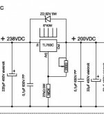
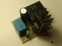
The implementation is simple, like the LM317. A protective zener diode (80-100V 5W) is required. In front of regulator I suggest a CRC and a transformer with a secondary 230VAC 0.15A (for 265V DC).
Attachments
Last edited:
Hi 🙂My prototype of the TDA1541A plays quite well, nice clean output
Time to buy out the whole eBay and rise the price of this DAC even more LOOL 🤣
- no digital filter, NOS
- full THT with glue-logic to maintain the nostalgia
- simultaneous mode (I2S input)
- big foil capacitors
- power supplies will be on the PCB (78/79xx regulators)
- opamps remain for the I/V
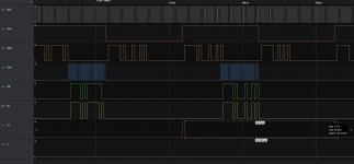
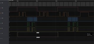
I am finishing some universal logic ICs I2S format interface to almost "every format".
Could be used for diskrete DAC R2R ladder too.
- data in the middle position between the LEs
- Stopped clock opperation
- MSB inverting option
- inverted data
- 14bit to 32bit word option
note in the datasheets that for TDA1540/41A TimeSim format
- BCK is inverted and conversion starts when 0 to 1 transition of LE
- MSB must be inverted
- BCK not inverted rising edge for MSB and conversion starts when LE going from 1 to 0.
_ MSB remains the same value
Attachments
Very nice Zoran, I was looking for a device like that for my TDA1540s. Many Thanks.
Ahaha, Miro didn't resist with the TDA1541A pcb .... one chip to rule them all. Ahaha we told him to stay away...now he will have to travel with it, bringing it back till the volcano forge of Mordor..under the mercantil eye of RyanJ...lol.
My TDA1541A pcb traces are made from elfique Myhtril, hardly extracted by dwarfs from the mountain... better than the copper. It litterally disseapers in the soundstage...invisible, yes. Ahaha but when a gobelin is in the room, then it shines! What a hobby 🙂
hi miro,
i am doing the pcb with stacked I2SoverUSB III and planning to use tube buffer for IV
if so, C29, C27, C28, C30, C31 and C34, C32, C33, C35, C36 are not needed to install?
Thank in advance
happy
In AD1865 DAC will i hear a difference if i replace C7,C8, C27, C28, C32, C33 Panaconic EEU-FC...330uF with Nichicon UFG...100uF not only because of the difference in uF?@happylistening Exactly, these capacitors are not needed for an external I/V 😉
Hi @happylisteningHi grunf,
I have bought the board from following link-:
https://www.diyaudio.com/community/...c85-6922-6dj8-etc-mu-follower-or-srpp.388295/
using 6N6P tube.
but I am struggling which HV power supply is good but easy (265V).
happy
Try the ECC88 instead, the 6N6 has a lower gain and is better as a buffer or line stage.Then the supply voltage will be lower (180V). I recommended the same to Vunce.
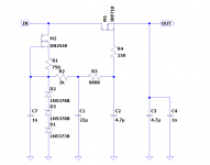
You can make a simple power supply or regulator according to this scheme, the sum of the zener diodes should be approximately the output voltage (Vzener=Vout + 4V) , I made it on a small PCB with smd resistors, the DN2540 can be in a TO92 case. M1 can be any n-mosfet for voltages higher than 400V and for lower currents .This reg is made for the ECC88 in my DAC.
You can also add protection diodes to M1 and a film cap of 2.2uF (or similar) to the input of the regulator.
Attachments
Amazing. Another great DAC design, that you also found time to build. Nice TDA1541a chip too 🙂
I hope you dont mind me asking the usual silly question: do you think you can hear differences in music intrinsic to the TDA1541a vs AD1862, despite all the differences in power and output stages?
It's too early to say, but I think AD1862 get nice competition. The battle will be very subjective and very interesting 🤣 ... this DAC has something in it, it really sounds nicely 👍
@Arnolddew
The size of the PCB is minimum: 190x90mm without power supply, or 190x150mm with power supply (can be more or slightly less). uf.l may be on the PCB.
Last edited:
@Zoran TDA1540 is slightly different from TDA1541A ... BCK is inverted for both, but TDA1541A must see the stopped BCK on the 0 (TDA1540 is 1), otherwise the LE is not accepted (this took me a few days to figure out because I used the BCK logic from TDA1540 and it did not worked even though the signals were aligned) 😉
I am surprised no one asked yet -- Will you post gerber files?It's too early to say, but I think AD1862 get nice competition. The battle will be very subjective and very interesting 🤣 ... this DAC has something in it, it really sounds nicely 👍
@Arnolddew
The size of the PCB is minimum: 190x90mm without power supply, or 190x150mm with power supply (can be more or slightly less). uf.l may be on the PCB.
@zoom777 of course I will do. My thread is the real deal for diy people, no bs 🤓
@happylistening
If you decide on TL783C, for 265VDC change 27k 5W to 33k 5W and trimmer 200ohm to 150ohm (or serial connection of 100ohm resistor & 50ohm trimmer).
If you decide on TL783C, for 265VDC change 27k 5W to 33k 5W and trimmer 200ohm to 150ohm (or serial connection of 100ohm resistor & 50ohm trimmer).
- Home
- Source & Line
- Digital Line Level
- DAC AD1862: Almost THT, I2S input, NOS, R-2R