
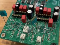
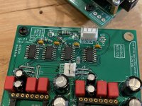
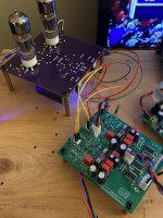
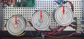
Stop-Clock MiroDac rev2.1 from post#3969 is alive. This board is set up for passive I/V (60R Rhopoint) feeding an SRPP 6n6p tube output stage.
https://www.diyaudio.com/community/...c85-6922-6dj8-etc-mu-follower-or-srpp.388295/
Jumpers were installed on the pcb in strategic places to direct the AD1862 Iout to the Molex output headers. Sockets installed for easy I/V resistor tweaking.
As Grunf pointed out in another thread, the amplification factor of the the 6n6p is low and not ideal for this application. To compensate for now, the preamp in the chain has bigtime voltage swing and gain.
https://www.diyaudio.com/community/threads/schade-common-gate-scg-preamp.380487/
I’m enjoying this setup very much 🙂
Thanks for sharing another project Miro!!
Attachments
-
 60D0AEB6-3F2A-4ED1-AD3A-BDC1F53BE20E.jpeg572.7 KB · Views: 260
 -
 A907639E-323E-466B-9F6D-275D84814CB3.jpeg515 KB · Views: 263
 -
 FEEE2DED-055A-4560-A7E7-E370BB97D2CE.jpeg611.8 KB · Views: 255
 -
 D1D10AAF-294B-45F2-B63F-3CF69A2362E0.jpeg620.6 KB · Views: 261
 -
 246E1108-AE40-49B8-B177-5A2DE529A5A5.jpeg495.8 KB · Views: 256

I would supress the 6n5p if the srpp gives enough output. (If what is showed is for a dac output stage)
Edit....ah had not read the previous post about cans amp.
Edit....ah had not read the previous post about cans amp.
Last edited:
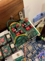
Its good to have fun designing and building something for yourself, but the boards linked below on aliexpress allow you to switch 2, 3, or 4 i2s lines via a button press, they are hardy in use, and you can set it up so that it neatly plugs on top of Miro's boards.
See this post for details https://www.diyaudio.com/community/threads/bluetooth.381383/#post-7052098
See this post for details https://www.diyaudio.com/community/threads/bluetooth.381383/#post-7052098
I don’t wish to derail this thread but…..
I want to add a coax connector to my Miro 1863 dac. Just so I can bypass the internal dac on my Onkyo cdp. At the same time I’d also like to add some rca connectors. How best to do this?
As always I appreciate your help
I want to add a coax connector to my Miro 1863 dac. Just so I can bypass the internal dac on my Onkyo cdp. At the same time I’d also like to add some rca connectors. How best to do this?
As always I appreciate your help
Coax is really just one hollow wire wrapped around a central wire. Carefully cut the outer insulation to expose the shield, then unwrap the shield. Cut the inner insulator to reveal the center conductor. Twist the shield back into a bundle and solder the two conductors to the board. Here's an example from a ham radio amplifier kit.

470R is too big, at least 100R or less for Riv. And don't touch the grid stoppers because the 5670 is a HF tube.I got a chinese 6N5P 5670 headphone amp on hand, can it good fit with RIV = 470R (the lowest I got on hand) as a tube buffer?
will the gain too big? (maybe need 100R to 200R?)
Thank you in advance for comment
I would perhaps play a little with working points of 5670, do you know how much current is through it?
I have changed the R IV to 50R. Thank you470R is too big, at least 100R or less for Riv. And don't touch the grid stoppers because the 5670 is a HF tube.
I would perhaps play a little with working points of 5670, do you know how much current is through it?
I bought 5670 tube headphone amp is a product. Sorry I didn’t measure the current


Nice! Just orderd the pcb's myself today. For the AD and the pcm63.I finally got around to putting my copy of Miro's great dac in a decent case. I used a 3U pesante from the DIYAUDIO store, plenty of room. Sounds great.
Yes this is more suitable value to match 5670. With Io=2mA p-p giving about 3.75Vp-p at the output in right phase.I have changed the R IV to 50R. Thank you
I bought 5670 tube headphone amp is a product. Sorry I didn’t measure the current
And maybe more important all of theese dac chips "prefer" more lower value of Riv. Someone long time ago measured distortion and current values, cant find the link in the forum 🙁
.
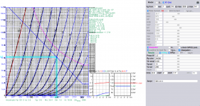
I used 5670 tube earlier in some audio applications and it was very good. And it is available and not so expensive. I attached some load line picture with datas and values.
Note that 5670 have 2 more linear regions, one in -1/-2V with lower anode voltages, another at -3.6V to -4V negative grid bias and higher anode voltages of 200V. This higher anode voltage is more suitable for tube because it is voltage device not current device...
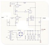
Classic 350-360V tube power supply. I made quick spice model for those willing to evaluate this tube.
.
The question of possible osculation is present because of small interelectrode capacitances. I add 0.7pF at each C node for socket-pin capacitance (as Norman Koren suggests). So the total dynamic capacitance in this circuit will be 2.9pF+(31.1+1)2pF=67pF
So this 67-70pF is already present in the circuit.
Idea is to make simple filter first with internal resistance of DAC (differ from each dac but available at datasheets with C parallel to Riv
And another with Rgrid and dynamic capacitance+optionaly another added real C. To combine Qfactors of that 2 stage HF filter for optimal phase shift and slope.
Baring in mind that NOS dac HF BW is 1/2Fs @2.xxx db (not sure avout exact value) so the filter should preserve given BW and Phase shift in HF. For this maybe the best way is to simulate circuit, and use some of HF online filter calcs. I simply dont see point of randomly choosing elements... 🙁
.
Another thing is a bit higher output resistance of the 5670 circuit because of slightly higher Ri of the tube. It is roughly 6K. And that will be an issue for eventual lower next stage potetntiometers or input resistors. For example some usual value of 10K for solid state devices will be hard load for this 6K output and some buffer will be a must... But maybe will be sufficient for higher input resistors of next stage like 470K or so. Anyway I think some tube buffer will be welcome,,,
.
Rk for Ug=-4V is about 650 ohm and shoul be bypassed with C to achieve the Gain. Value of that Ck is in conjunction with C in power branch to Rload and anode. And this is with Cout which value is strongly connected with next Rinput forming LF behavior and could be act as LF and bass cut-off.
Sorry for lonfer post but this 5670 reminded me for using this tube as input stage in some SE amp i made decades ago 🙂
.
** 5670 ****************************************
- Created on 08/21/2022 20:25 using paint_kit.jar 3.1
- www.dmitrynizh.com/tubeparams_image.htm
- Plate Curves image file: GE 5670 datas
- Data source link:
.SUBCKT 5670 1 2 3 ; Plate Grid Cathode
+ PARAMS: CCG=2.9P CGP=2P CCP=1.7P RGI=2000
* added 0.7pF to each node for socket-pin capacitance
+ MU=35.7 KG1=975 KP=158 KVB=66 VCT=0.07 EX=1.61
- Vp_MAX=325 Ip_MAX=14 Vg_step=1 Vg_start=1 Vg_count=10
- Rp=24000 Vg_ac=0.08 P_max=1.5 Vg_qui=-4 Vp_qui=200
- X_MIN=44 Y_MIN=56 X_SIZE=609 Y_SIZE=657 FSZ_X=1476 FSZ_Y=812 XYGrid=true
- showLoadLine=y showIp=y isDHT=n isPP=n isAsymPP=n showDissipLimit=y
- showIg1=n gridLevel2=n isInputSnapped=n
- XYProjections=y harmonicPlot=y dissipPlot=y
E1 7 0 VALUE={V(1,3)/KP*LOG(1+EXP(KP*(1/MU+(VCT+V(2,3))/SQRT(KVB+V(1,3)*V(1,3)))))}
RE1 7 0 1G ; TO AVOID FLOATING NODES
G1 1 3 VALUE={(PWR(V(7),EX)+PWRS(V(7),EX))/KG1}
RCP 1 3 1G ; TO AVOID FLOATING NODES
C1 2 3 {CCG} ; CATHODE-GRID
C2 2 1 {CGP} ; GRID=PLATE
C3 1 3 {CCP} ; CATHODE-PLATE
D3 5 3 DX ; POSITIVE GRID CURRENT
R1 2 5 {RGI} ; POSITIVE GRID CURRENT
.MODEL DX D(IS=1N RS=1 CJO=10PF TT=1N)
.ENDS 5670
*$
Attachments
Does anyone notice a difference between the USB cables on these DACs? The more silver the better it plays...I just put in a shorter cable and it plays even better than the longer one. I know it's all ones and zeros here but this is amazing. 🤣
That may possibly be due to different 'antenna' characteristics of the two USB cables because they are of differing loop-area. While such RF antenna pick-up effects are not enough to change 1s to 0s, or 0s to 1s they might be enough to audibly alter the DAC's conversion clock-jitter. Another, although I suspect a lesser, possibility is that the shorter cable is allowing less ground noise introduction via the USB interface. Without going into details, that has to do with in-home radiated power mains frequency pick-up, and also with the D.C. resistance of the cable's conductors.Does anyone notice a difference between the USB cables on these DACs? The more silver the better it plays...I just put in a shorter cable and it plays even better than the longer one. I know it's all ones and zeros here but this is amazing. 🤣
In a digital only system, clock-jitter is of no consequence, just as you would think. Unless, of course, it is so severe as to provoke actual bit reading errors at the receiving end. Which would require microsecond levels of jitter for CD rate data-transfer. In a mixed-signal system like a DAC, clock-jitter corrupts the short-term stability of the clock controlling the quantizer conversion instant, which then manifests as an uncorrectable analog error post the D/A conversion.
Last edited:
Nicely built.I finally got around to putting my copy of Miro's great dac in a decent case. I used a 3U pesante from the DIYAUDIO store, plenty of room. Sounds great.
Don't forget to insulate the top nut from the hood.
Otherwise, you may create a virtual extra winding on the torroid transformer, causing it to burn out.
Attachments
- Home
- Source & Line
- Digital Line Level
- DAC AD1862: Almost THT, I2S input, NOS, R-2R