Yes, I'll test it.For raspberry it is the best to use USB card to do the I2S job 👍
1. Raspberry Pi4, USB2 port ->JLSounds card ->AD1865 DAC (JLSounds card connected directly to AD1865)
Can you test this?
Raspberry Pi4, USB2 port ->JLSounds card ->AD1865 DAC with shift registers
And further test very cheap USB-I2S - PCM2706 with raspberry?

I'm using Charcroft Z-Foil resistors.Can you tell me the product name of the passive I/V resistor? It looks like a Caddock in the picture.
https://www.hificollective.co.uk/components/car_resistors.html
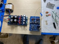
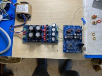
Progress,H5.J4 wire jumper is ok
A1 and A2 without resistors
SJ3 just a solder blob
Please look at the pictures and advise.
This configuration is for test only but I do intend to mount components to a board. How should I ground the power supply and dac?
Thanks
I’ve verified correct output from psu1
Attachments
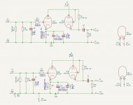
I have attached the schematic:@gaszto Could you share the schematics of the tube output stage please?
B+ voltage 180-220 V DC
Heater voltage 6.3 V DC
Attachments
I am certain that when you try out the pcm56, you wont regret it. It sounds weightier and very fluid.I've got myself some PCM56 and the required boards...see how they compare to the '62 when I get round to building!
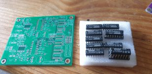
Have spare boards and 4 chips if any interest.
I have attached the schematic:
B+ voltage 180-220 V DC
Heater voltage 6.3 V DC
I have attached the schematic:
B+ voltage 180-220 V DC
Heater voltage 6.3 V DC
Hi gaszto,
I plan to connect the miro AD1862 to the tube stage instead of your AD1865 HAT. I have a question about this circuit you shared.
1) It is expected that R1 and R2 of AD1865 HAT are passive i/v resistors. The resistance value is printed on the PCB saying 100 ohms, is this value correct? Is this value valid for AD1862 as well?
2) AD1862 does not currently have a passive i/v resistor, so a 100 ohm resistor must be connected. There is no place to mount it on the DAC board. Can I use a 100 ohm resistor (passive i/v) for R3_1 and R3_2 marked as optional on the tube stage?
3) Is R2,R7 680R for reducing the signal? What is it for?
Thank you.
Hi,Hi gaszto,
I plan to connect the miro AD1862 to the tube stage instead of your AD1865 HAT. I have a question about this circuit you shared.
1) It is expected that R1 and R2 of AD1865 HAT are passive i/v resistors. The resistance value is printed on the PCB saying 100 ohms, is this value correct? Is this value valid for AD1862 as well?
2) AD1862 does not currently have a passive i/v resistor, so a 100 ohm resistor must be connected. There is no place to mount it on the DAC board. Can I use a 100 ohm resistor (passive i/v) for R3_1 and R3_2 marked as optional on the tube stage?
3) Is R2,R7 680R for reducing the signal? What is it for?
Thank you.
1.) According to the datasheets AD1865 and AD1862 have the same +/-1mA output (2mA peak to peak). If we are using 100R resistor as the I/V resistor, the output voltage will be U=R*I=100R*0.002A=0.2V (peak to peak). The gain of this "bypassed" SRPP stage is around 23. 0.2V*23=4.6V (peak to peak)-> 1.626 Vrms.
I'm using 100R resistor because the output level is matched with my tube phono stage, there is no volume difference if I changing the source from DAC to Phono.
Theoretically the I/V resistor is connected parallel with the AD chip R2R resistor network, so theoretically the sound is improving if you are using smaller resistance. But of course you will have smaller output signal.
2.) Yes, you can definitely place I/V resitors in the R3_1 and R3_2 position. I made this,because I used a transformer between the DAC and the Output Stage and I placed the I/V resistor at the secondary side of the transformer, according to sowter!s recommendation.
https://www.sowter.co.uk/dacs.php
3.) R2 and R7 are gridstopper resistors. It helps prevent high frequency parasitic oscillation in the tube.
Usually the value of this resistor is 1.5K or 5.6K. With the tube capacitance it is forming a low pass filter. But for example, using 3K resistor in this position is lowering the signal level, and add lots of noise (resistors Johnson-noise are correlating with the resistance). If we are adding a capacitor (C5 and C6) paralell with the tube capacitance, we can use smaller resistance values. You can use different values, but you have to change the C5 and C6 too.
Here is how to calculate it:
http://www.valvewizard.co.uk/gridstopper.html
Hi,
1.) According to the datasheets AD1865 and AD1862 have the same +/-1mA output (2mA peak to peak). If we are using 100R resistor as the I/V resistor, the output voltage will be U=R*I=100R*0.002A=0.2V (peak to peak). The gain of this "bypassed" SRPP stage is around 23. 0.2V*23=4.6V (peak to peak)-> 1.626 Vrms.
I'm using 100R resistor because the output level is matched with my tube phono stage, there is no volume difference if I changing the source from DAC to Phono.
Theoretically the I/V resistor is connected parallel with the AD chip R2R resistor network, so theoretically the sound is improving if you are using smaller resistance. But of course you will have smaller output signal.
2.) Yes, you can definitely place I/V resitors in the R3_1 and R3_2 position. I made this,because I used a transformer between the DAC and the Output Stage and I placed the I/V resistor at the secondary side of the transformer, according to sowter!s recommendation.
https://www.sowter.co.uk/dacs.php
3.) R2 and R7 are gridstopper resistors. It helps prevent high frequency parasitic oscillation in the tube.
Usually the value of this resistor is 1.5K or 5.6K. With the tube capacitance it is forming a low pass filter. But for example, using 3K resistor in this position is lowering the signal level, and add lots of noise (resistors Johnson-noise are correlating with the resistance). If we are adding a capacitor (C5 and C6) paralell with the tube capacitance, we can use smaller resistance values. You can use different values, but you have to change the C5 and C6 too.
Here is how to calculate it:
http://www.valvewizard.co.uk/gridstopper.html
Thanks for the detailed reply. it will be a lot of help.
I've got myself some PCM56 and the required boards...see how they compare to the '62 when I get round to building!
Coincidentally I just did the same and fired it up this morning. Be interested to hear what your ears think.
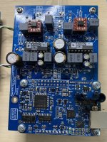
Shall be a little while yet for me Paddy. Albeit I did manage to solder in the shift registers this morning. Going to try something a bit different for the power. Thinking some stiff but unregulated capmx types. And maybe into a D1 IV. So it won't be a fair comparison to my 1862!
That should be super nice!
Don't forget the 16/18 bit jumper, I spent an hour debugging something that would have been nothing if I'd actually read the instructions. Forgetting J13 didn't help either.
Mine is built identical to my 1862, excepting for fancy GR IV resistors but previous experiments showed the Vishay metal films didn't give up much to them.
Initial reaction is that it's very listenable and nicely detailed, but so far not better than the 1862. Kind of like the 1865: very nice if you can't get 1862 chips, but we don't have that problem here 🙂
I have a few boards and new Rochester-sourced BB chips on this side of the pond, PM me if you're in north America else buy Jim's.
Yes I saw the jumper today....it jogged my memory! I've also got some of those small psu boards by @Traktorist3d, the 317/337 with smd transistors. Should be interesting.
I have a load of those tiny boards if anyone wanted to try.
I've potentially earmarked 4 56ks for someone.
I have a load of those tiny boards if anyone wanted to try.
I've potentially earmarked 4 56ks for someone.
I have new Rochester-sourced BB chips on this side of the pond ....
K grade ?
Patrick
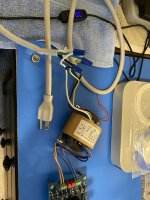
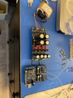
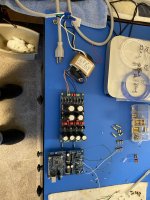
Slow progressProgress,
Please look at the pictures and advise.
This configuration is for test only but I do intend to mount components to a board. How should I ground the power supply and dac?
Thanks
I’ve verified correct output from psu1
Attachments
- Home
- Source & Line
- Digital Line Level
- DAC AD1862: Almost THT, I2S input, NOS, R-2R