@Hidy
You can build 4 PCBs and drive them together from one I2S source and parallel current outputs to one opamp output. You can achieve better result as with stacking chips 🙂
Well, it can also goes with more timing error issues too ... as different ground loops!
 (spaghettis wires is not wanted)
Last edited:
He can hold one size for all LRCK wires and center GND in one spot (all signal wires are going to the I2S source) 
Btw, I'm wondering how it works whith the data channel ? I mean this chip was used with a filter chip before. Do you think the R&L data channel was demultiplexed and sent to each channel or both channel receive the I2S data multiplexed and know the good rank because the Lrck ????
I ask because with the TDA1541 there is a 4 channel demultiplexed mode for the data and it sounds way better than the I2S option (you can choose either). Don't ask me why it sounds better that way cause anyway the timing must be right whatever the data channel is multiplexed or splited in two channel ?! If possible in spite of adding more dac chips which is going to more jitter whatever the lrck length for each (because the intrinsec jitter difference between factory batches of the dac chip itself at reading ECDESIGNS long TDA1541 thread), perhaps better to work on a segmented L&R data channel ???
There is also Iancanada who made a I2StoPCM board AD1862 compatible but I beleive it still a standalone multiplexed data channel sent to each ad1862 chip, so two wires but the same I2S data multiplexed sent on each wire.
Btw, FGPA having themselves jitter I really don't know if the idea of demultiplexing is easily feasible or simply a goode one ?!😕🙄 (but works darn good with the TDA1541A VS simple I2S)
A question maybe to ask to JLSOUNDS as they use a FGPA I assume for all the chips options...
I ask because with the TDA1541 there is a 4 channel demultiplexed mode for the data and it sounds way better than the I2S option (you can choose either). Don't ask me why it sounds better that way cause anyway the timing must be right whatever the data channel is multiplexed or splited in two channel ?! If possible in spite of adding more dac chips which is going to more jitter whatever the lrck length for each (because the intrinsec jitter difference between factory batches of the dac chip itself at reading ECDESIGNS long TDA1541 thread), perhaps better to work on a segmented L&R data channel ???
There is also Iancanada who made a I2StoPCM board AD1862 compatible but I beleive it still a standalone multiplexed data channel sent to each ad1862 chip, so two wires but the same I2S data multiplexed sent on each wire.
Btw, FGPA having themselves jitter I really don't know if the idea of demultiplexing is easily feasible or simply a goode one ?!😕🙄
(but works darn good with the TDA1541A VS simple I2S)A question maybe to ask to JLSOUNDS as they use a FGPA I assume for all the chips options...
Last edited:
@diyiggy
TDA1541 has direct I2S option (the logic inside chip does the conversion), second option is demultiplexed mode.
AD1862 is only demultiplexed (this is why shift registers are needed for I2S), output state is drived by LRCK (data are clocked with BCK into internal buffer and then written with LRCK on the output). As you can see, only LRCK jitter depends for this chip. LRCK is not affected by the shift register logic because is feeded directly from I2S source 🙂
I let the question about FPGA and jitter opened, because IDK the final answer ... I only know, that I did not find sound difference between xmos (very low jitter directly without fpga) and PCM2706 (500ps jitter) 😀
Thank you M,
I would have noticed that by a closer look to your shematic. So I maybe had a conclusion in the wrong direction, so maybe that is the I2S internal logic of the TDA1541 that is less good than today fast external registers and so off topic regarding a possible improvement way for the AD1862.
There must be something too with those two parts dac chips perhaps...as for the TDA1540 ...humm I don't know. Too many dac chips and still two ears only.
I only know, that I did not find sound difference between xmos (very low jitter directly without fpga) and PCM2706 (500ps jitter) 😀
So after this an EasyDAC with proper (separated from USB source) PSU should sound almost similar to the desktop AD1862 dac with XMOS USB.
Up to now I was not enough motivated to make a split cable for that.
Cheers, Ernst
@Ernst
Compactness of EasyDAC is the main aspect why it was born. The main difference is in components (different capacitors) and power supplies 🙂
Compactness of EasyDAC is the main aspect why it was born. The main difference is in components (different capacitors) and power supplies 🙂
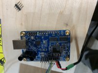
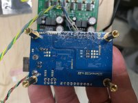
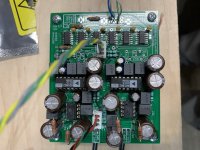
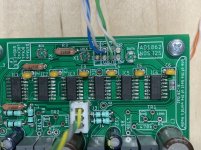
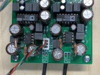
I finally got all the pieces and parts for my DAC, but I’m getting no sound. I’m using the I2SoverUSB v.III and have it configured like the description in post #617. I’m also powering the digital side with an external 5vdc source. I’m using the 1.3 if.l board with the 74AHCT164D shift registers. My source computer is a Raspberry PI 4B running Volumio, and the app sees the I2SoverUSB.
Any advice on troubleshooting would be very helpful.
Since I have extra boards, I’m thinking about building the DAC without the shift registers to see if I can get it working.
Any advice on troubleshooting would be very helpful.
Since I have extra boards, I’m thinking about building the DAC without the shift registers to see if I can get it working.
Attachments
-
 061682E3-08E3-4882-A8F6-F2714FE2675B.jpeg293.1 KB · Views: 460
 -
 287D0C60-99FB-4D4F-A6BD-E9E16FC5578B.jpeg299.2 KB · Views: 426
 -
 4C8FEE8B-6A8E-47A3-8BD9-44DC7D4BB289.jpeg483.6 KB · Views: 411
 -
 9AAD0752-C671-45EE-A01F-17D5009EAF5D.jpeg374.8 KB · Views: 422
 -
 6B2D4016-6C88-4E4A-8D84-EF648E964A6D.jpeg308 KB · Views: 399
@BRN First make it working on your PC or laptop, then go with raspberry 🙂
The connection and jlsounds configuration seems be fine.
The connection and jlsounds configuration seems be fine.
Bring it by and we can take a look on my scope. I've got some experience with errors on the shift registers...
Might try reflowing the solder on those chips, several pins look a little skimpy.
Might try reflowing the solder on those chips, several pins look a little skimpy.
Last edited:
Ed,
Thank you. Let me play with a little more and see if I can figure it out.
That could be the case. I have two options. One reflow the solder on the shift registers and build another board without them and reconfigure the I2SoverUSB to feed the AD1862 directly.
Thank you. Let me play with a little more and see if I can figure it out.
That could be the case. I have two options. One reflow the solder on the shift registers and build another board without them and reconfigure the I2SoverUSB to feed the AD1862 directly.
@BRN You can use the simplest probe for digital signals: LED diode with 1k resistor or a buzzer 
Use this LED to see if BCK, LRCK, DR, DL are present on DAC pins while the music plays. DR or DL will shine only when the music is active, so be sure the music is on
You can trace pins and find the problem.
Use this LED to see if BCK, LRCK, DR, DL are present on DAC pins while the music plays. DR or DL will shine only when the music is active, so be sure the music is on
You can trace pins and find the problem.
Last edited:

- Home
- Source & Line
- Digital Line Level
- DAC AD1862: Almost THT, I2S input, NOS, R-2R