Hmmmm....I thought that quote was only referring to an implementation using 100Ω resistors instead of the datasheet 240Ω ones.....Back in post #257 Elvee suggested that the 33R resistors were not necessary in this implementation so I left them out.
In any case, THANK YOU for taking the time to do this layout!
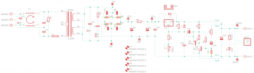
10nF is the final recommended value for a standard 317.Elvee, with the LM317 de-noiser boards, did you decide on 10nF or 15nF comp caps? I seem to remember you later on going to the larger value to avoid oscillation with no performance penalty.
The 337 is slightly less stable, but 10nF is still OK.
For other types, different values and/or the resistor might be needed.
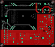
It’s morning and not enough coffee circulating my blood streambut BC337 pads seems to be right. Pin 1 is collector and it is connected to the R6. Pin 3 emitter is connected to the ground.
As for R2, there is no place for higher power rating resistor. I will use 2W. RC filter is not primary for increasing PSSR at 100 Hz but for maintaining good PSSR at higher frequencies, thus filtering HF noise from rectifier and mains.
One additional note: MUR 120 diodes are good up to 300 – 400 mA load. For higher current I would use SBYV27-200 diodes.
Cheers for checking Tombo. Seems to be just my Eagle Library. Need to update!
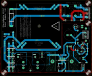
Please go easy, this is my very first board in about fifteen years. Things have changed a lot since then eh!? Anyway, was a nice project to learn Eagle. As well as Tombo's off-board transformer layout, I also needed a single rail on-board PCB for other projects (linear PSU for DACS etc). So I had a spare few hours and came up with this.
Using Nisbeth's STEPS layout (with prior permission) as a baseline, it incorporates:

I think I may need some feedback:
Is this the best way to implement the ground plane and Kelvin connections? I was very confused despite reading about it for a couple of hours!
Is the mains & bridge suppression a bit overkill?
Can someone double check my transistor pinouts. I had trouble with Eagle giving me wrong information.
General thoughts before V2 and Gerbers.
A huge load of thanks to:
1) Nisbeth for the baseline LM317 layout, who borrowed elements from Warren Young's STEPS: theslowdiyer | DIY electronics and audio projects – at a snail's pace! I have adapted with prior permission.
2) Elvee and Diego for their inspiration and technical genius in this. Are there any downsides of this versus standard LM317 schematic?
3) Tombo for troubleshooting the BOM components and general silly queries
Using Nisbeth's STEPS layout (with prior permission) as a baseline, it incorporates:
- X and Y mains suppression and choke.
- Transformer snubber (CRC).
- Onboard Talema style PCB transformer with pins for 5VA to 25VA.
- 230-240V, secondaries in parallel. Version 2 will have selectable jumper pads for primary and secondary windings.
- TO-220 packaged bridge diodes with noise supression caps (overkill?).
- Up to 2x10,000uF filter caps via a pi-filter (CRC).
- Elvee/Diego Sziklai Pair Die-Noizator.
- Kelvin connections (I think?).
- LED for minimum current draw.
- Fits 120x100mm Hammond 1455N12 case. AC receptacle space above VOUT terminal.
- Onboard acknowledgements to Nisbeth, Elvee, Diego, Warren Young.
- Gerbers to be released for V2 following comments.
I think I may need some feedback:
Is this the best way to implement the ground plane and Kelvin connections? I was very confused despite reading about it for a couple of hours!
Is the mains & bridge suppression a bit overkill?
Can someone double check my transistor pinouts. I had trouble with Eagle giving me wrong information.
General thoughts before V2 and Gerbers.
A huge load of thanks to:
1) Nisbeth for the baseline LM317 layout, who borrowed elements from Warren Young's STEPS: theslowdiyer | DIY electronics and audio projects – at a snail's pace! I have adapted with prior permission.
2) Elvee and Diego for their inspiration and technical genius in this. Are there any downsides of this versus standard LM317 schematic?
3) Tombo for troubleshooting the BOM components and general silly queries
Attachments
Last edited:
Quick question (probably been answered before already): are precautions for minimum current draw really necessary with the LM317? The de- or die-noiser already draws a couple of mA, together with a reasonable dimensioned R1 there should be more than the 5 mA minimum regulator current (in most cases).
I think I may need some feedback:
Ah, you know how to catch your fish
Caps in parallel with fast recovery diodes are not necessary. Instead of suppressing, while diode transitions to reverse voltage, they discharge and produce some switching noise.
I personally don’t like LED diode on the output of ultra low noise power source as LED diodes are practically noise generators.
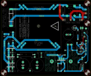
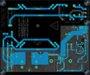
Current carrying traces (force) are unnecessary thin. There is place to make them thicker starting from C7 to the regulator and all way long to the output connector.
Kelvin connection is present on this design but I would move origin points to the output connector pins.
BC327/BC337 pads are oriented/connected right.
My personal opinion is that mains suppression is not overkill but must. It can be on the PS board or in the power entry module (Schurter module).
Ah, you know how to catch your fish
Caps in parallel with fast recovery diodes are not necessary. Instead of suppressing, while diode transitions to reverse voltage, they discharge and produce some switching noise.
I personally don’t like LED diode on the output of ultra low noise power source as LED diodes are practically noise generators.
Current carrying traces (force) are unnecessary thin. There is place to make them thicker starting from C7 to the regulator and all way long to the output connector.
Kelvin connection is present on this design but I would move origin points to the output connector pins.
BC327/BC337 pads are oriented/connected right.
My personal opinion is that mains suppression is not overkill but must. It can be on the PS board or in the power entry module (Schurter module).
That's awesome! Thanks so much. Definitely needed another pair of eyes. Will implement those changes after a few more people's comments.
I still don't get the Kelvin connections though. Does R4 need to be within sense or connected to force? I really did have a read, I promise! It's just tricky to appreciate how to apply it here. Presumably the whole section outside the normal LM317 schematic (i.e. "the add on") is within the voltage sense area? If so, I'll need to have a head scratch about this. Will it make a massive difference?
About the LED: I thought one LED wasn't going to make such a huge difference? I read it was mainly an issue when multiple/arrays are used. I was hoping it would be below the noisefloor, but I could be wrong.
With the denoiser, the 5mA requirement is met easily.Quick question (probably been answered before already): are precautions for minimum current draw really necessary with the LM317? The de- or die-noiser already draws a couple of mA, together with a reasonable dimensioned R1 there should be more than the 5 mA minimum regulator current (in most cases).
Very nice job!That's awesome! Thanks so much. Definitely needed another pair of eyes. Will implement those changes after a few more people's comments.
I still don't get the Kelvin connections though. Does R4 need to be within sense or connected to force? I really did have a read, I promise! It's just tricky to appreciate how to apply it here. Presumably the whole section outside the normal LM317 schematic (i.e. "the add on") is within the voltage sense area? If so, I'll need to have a head scratch about this. Will it make a massive difference?
About the LED: I thought one LED wasn't going to make such a huge difference? I read it was mainly an issue when multiple/arrays are used. I was hoping it would be below the noisefloor, but I could be wrong.
The connection of R4 does not matter in practice, but in theory placing it as close to the regulator as possible would be preferable (don't do tradeoffs to achieve it: it is not worth the trouble).
The LED will not cause troubles, since it has a series resistor. People can omit it if that is their preference.
A final remark: the traces of the mains-connected Y caps are a bit too close to the low voltage side for my personal comfort.
The clearances/creepage distances might be OK, but I would try to increase them if possible
I personally don’t like LED diode on the output of ultra low noise power source as LED diodes are practically noise generators.
That's not right in this generalization. Bright blue LEDs can be nearly as bad
as an unaided LM317.
Some red LEDs such as HP -> Avago -> Qorvo??? HLMP6000 are about as
low noise as it gets:
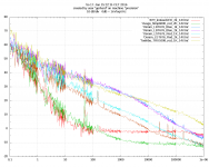
0 dB = 1nV/rtHz at 100 Hz,
-10 dB = 320 pV/rtHz @ 2 KHz.
You won't get a much quieter reference without filtering.
The limit at LF is my amplifier. LEDs are fed with 2K wire resistor from 14V NiCd.
Replacing them with a 47 Ohm resistor results in slightly less than 1nV/rtHz,
as should be. That also means that the batteries do not inject noise.
The boards for my new amplifier are in the mail from China. New measurements
are to be expected RSN.
Gerhard
Attachments
Last edited:
Ah, you know how to catch your fish
Caps in parallel with fast recovery diodes are not necessary.
Current carrying traces (force) are unnecessary thin.
Kelvin connection is present on this design but I would move origin points to the output connector pins.
The connection of R4 does not matter in practice, but in theory placing it as close to the regulator as possible would be preferable (don't do tradeoffs to achieve it: it is not worth the trouble).
A final remark: the traces of the mains-connected Y caps are a bit too close to the low voltage side for my personal comfort.
The clearances/creepage distances might be OK, but I would try to increase them if possible
Thanks to both of you. Here's V1.1 with the above addressed. Going to read up a bit moire about the bridge caps. It has been a nice little first project to learn Eagle. Went full force on the output rail! Elvee's comment about R4 really helped, and it meant that I was able to remove a trace going through the ground plane. Win-win. Thanks for the info about the low-noise LED Gerhard.
Would welcome comments/thoughts. Trying to aim for a no-compromise design.
Attachments
Last edited:
That's not right in this generalization.
It is very helpful to see measured facts instead of my theoretical opinion.
You have nice measurement gear.
Last edited:
How BIG is this board?Here's V1.1 with the above addressed.
“cdsgames” is user on this forum and from company Allo, producers of Boss, Katana and Revolution DACs (IDK if owner or/and chief designer). They also produce dedicated LPS for their DACs. He said that he will test denoiser designs with LDO regulators and report back.
Yes I will have test results in about 1 week
How BIG is this board?
Should be 3.95” x 4.7” (app. 100 x 119 mm) - it doesn't look like it's been changed at least.
Note that my original layout was intended to slide into a Hammond 1455-style case, but unfortunately the primary pins on the transformer are much too close to the bottom plate to really allow this - you'll need something bigger.
Andy - nice job on the changes
...and a bit more nitpicking
- The mounting pad near the output connector doesn’t really do anything so you can get rid of that if you want to (it was supposed to be for mechanical support if the board was put into the hammond case but as mentioned above that isn't possible anyway).
- From the schematics I have seen the C12 cap is only 100uF? If so, that footprint is a bit larger than it needs to be (ø10 should be OK)
- If you don’t need the meter connection, removing it will be OK (you can still wire a meter to the output).
- If the red trace marked N$5 is joined to the blue trace at the top, you can do that at the transformer pin and save a via.
- You might be able to clean up the area around R6/C11 by putting R6 parallel to the edge of the board and then turning C11 around to shorten those traces.
...and a bit more nitpicking
- The mounting pad near the output connector doesn’t really do anything so you can get rid of that if you want to (it was supposed to be for mechanical support if the board was put into the hammond case but as mentioned above that isn't possible anyway).
- From the schematics I have seen the C12 cap is only 100uF? If so, that footprint is a bit larger than it needs to be (ø10 should be OK)
- If you don’t need the meter connection, removing it will be OK (you can still wire a meter to the output).
- If the red trace marked N$5 is joined to the blue trace at the top, you can do that at the transformer pin and save a via.
- You might be able to clean up the area around R6/C11 by putting R6 parallel to the edge of the board and then turning C11 around to shorten those traces.
Thanks Nisbeth. Will take a look at those points and see whether I can address them.
About the Hammond case, I've moved the transformer south by 3mm, giving 5mm between board edge and transformer casing. The Hammond slot depth is 2.5mm. Still not idea, and there is scope to move this even further.. However, there will be no space to place jumper pads for Primary & Secondary customisation. However, safety trumps. As a reference, my old Warren Young STEPS 1.0 was 2mm gap!
Versus the minimum safety standard, this seems enough: PCB Trace Spacing Calculation for Voltage Levels
Last edited:
The on-board clearances are not the problem, they've tested good already and there's room room do more if you want. Also, 230/115V switching was not a priority to me - I just did two board versions
The problem is that the Hammond case has a round bit in the corner (where the screws go) so if you look at it "in 3D" there's less clearance between the bottom of the board and the bottom/side of the case than you expect when you just look at the drawing. You can't raise the board up because then the heatsink doesn't fit. A 25mm heatsink and a 10/15VA transformer in the tall case version would work, but there was not space for the "full fat" version with a 25VA transformer and a bigger HS.
It's definitely possible that what you have done is enough and otherwise you can probably fix it, but I just did not realise it was a problem until I slid my finished prototype board into a Hammond case and realised there was no way that was going to be safe for 230V in an all-metal case. I was pretty happy with the layout otherwise so picking a different case was easier than ripping the whole thing apart again
- Home
- Amplifiers
- Power Supplies
- D-Noizator: a magic active noise canceller to retrofit & upgrade any 317-based V.Reg.