Something must be feeding those gates - gate stoppers form a RC loop with the gate, so at DC you shouldn't experience any difference when changing gate stoppers. As far as I recall, the distance from gate stopper to gate is quite short and the longer trace is on the other side.
Last edited:
Little update:
taking out the current current limiting resistors and bjt actually did something, will take out the fets and match at higher currents to make sure they are allright.
On a sidenote: The transforrmer stopped humming, i am prettty sure there was (or still is) oscillation. Now diner and then back to the bench.
Something must be feeding those gates - gate stoppers form a RC loop with the gate, so at DC you shouldn't experience any difference when changing gate stoppers. As far as I recall, the distance from gate stopper to gate is quite short and the longer trace is on the other side.
as far as i recall with larger 177 Ohm gatestoppers the situation was seriously worse. I removed the current limiting circuit and will now reassemble everything for more testing, maybe we reached the point where i can put some square waves through later this evening.
...i am prettty sure there was (or still is) oscillation...
If you have, this should find it.
Its more sensitive than the LED one, but you do need to use germanium detector/demodulation diodes.
CAUTION
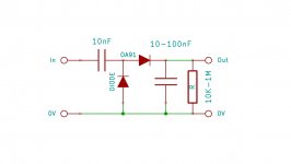
The OA91's are rated to 10V, an input spike more than that will kill the diodes, clamp it with a some zenners.
Attachments
And now i got -0.450V offset with both pots set to zero, i guess one of the jfets died 😡
Last edited:
And now i got -0.450V offset with both pots set to zero, i guess one of the jfets died 😡
Jfets and cascode BJTs were desoldered and checked. They test fine, anybody got a clue what could have gone wrong? I still have 0.45V offset with he pots turned all the way down. P2 does not seem to do anything anymore now.
with pots on zero , you can't expect anything to be in any ballpark
P1 and P2 - you need plenty of turns from zero to start seeing any change in mosfet conduction
anyway , check everything , put back , and start again
this time , use your editing skills - post schematic with some measurements and post some pictures of your build
we are in blind here , without that
P1 and P2 - you need plenty of turns from zero to start seeing any change in mosfet conduction
anyway , check everything , put back , and start again
this time , use your editing skills - post schematic with some measurements and post some pictures of your build
we are in blind here , without that
A word of caution regarding P1/P2 - I have witnessed many burned circuits due to turning one of them all the way open without any measurable effect and then something suddenly starts pulling current and then smoke...
Get a bunch of cheap DMMs and make sure to measure at a minimum both the N and P side of the push-pull as you slowly crank up both P1 and P2 (quarter or half turn on-by-one).
Get a bunch of cheap DMMs and make sure to measure at a minimum both the N and P side of the push-pull as you slowly crank up both P1 and P2 (quarter or half turn on-by-one).
this time , use your editing skills - post schematic with some measurements and post some pictures of your build
we are in blind here , without that
Right on ZM!
And I'll add improved vision by posting the schematics and board layout - sorry for not doing it much sooner. 😱


Right on ZM!
And I'll add improved vision by posting the schematics and board layout - sorry for not doing it much sooner. 😱
View attachment 706110
View attachment 706111
Ah great, many thanks cviller! That was definitely needed. I took everything apart, all semiconductors seem ok. I will put it back together and take measurements. I hope i still got my microsof paint skills.
Yes S74 was soldered in wrong, got it fixed, still roughly 315mV offset at the output. Measuring around 4mV across the source resistor of Q104 it seems that this little bastard is conducting a tiny amount of current. Q4 on the other hand does not.
4mv thats right around 8.5mA ... thats the IDSS of the Jfets.. hmmm could it be that the Mosfet Q104 is blown?
4mv thats right around 8.5mA ... thats the IDSS of the Jfets.. hmmm could it be that the Mosfet Q104 is blown?
Last edited:
With the other Mosfett installed i see no traces of current draw in the mosfets anymore. With the pots set to 0 still get 48mv offset.
I lifted a pad of the gate resistor. I had enough of this pos, i gonna scrap that thing, one week wasted troubleshooting, really i had enough 😡
I lifted a pad of the gate resistor. I had enough of this pos, i gonna scrap that thing, one week wasted troubleshooting, really i had enough 😡
Jour transistors are genuine from trusted sources ?
Pattience You do enjoy music more after efforts 😉
Good luck!
Pattience You do enjoy music more after efforts 😉
Good luck!


With the other Mosfett installed i see no traces of current draw in the mosfets anymore. With the pots set to 0 still get 48mv offset.
I lifted a pad of the gate resistor. I had enough of this pos, i gonna scrap that thing, one week wasted troubleshooting, really i had enough 😡
Don't worry about offset before you have some current through the push-pull output.
Don't worry about offset before you have some current through the push-pull output.
Well lets mount her on the heatsinks and fire her up. I really dont mind if blows up at this point. I know you are in the process of moving but could you send one or two replacements boards cviller?
Razorblade,
Thanks for posting the details of your troubleshooting! We're wishing you good luck with this F5!
Thanks for posting the details of your troubleshooting! We're wishing you good luck with this F5!
Things are looking a little better now. Here is the daily report:
The state of the amp is back back to were we started. Matched fets from a forum member, 47 ohm gatestoppers, basically the only difference is that the current limiting circuitry has been removed
Its cooking now at 1000mA per device, target is 1250 mA. I want 100W Class A into 6 Ohm. Voltages across the current sense resistors are:
N-Channel: 491mV and 535mV
P-Channel: 509mv and 509mV
the P-Channel is still way better matched but the huge difference we had at the beginning is gone now. I will contact the seller of the mosfets and le him investigate. Do you think the difference is acceptable I think about ordering a batch of P and N Channel devices from digikey and match some myself. I will check this channel with he signal gen tomorrow and see how the square wave response looks, i will remove the current limiting circuit of the other working channel tomorrow too and have a closer inspection on its voltages across the source resistors, but as far as i recall they were ultra close.
Whats important to note: its now Q4 that has the higher voltage across the source resistor. before it was always Q104 no matter which of the mosfets were in the position.
And we might have one dead Mosfet (stll have to check), the replacement one from my parts bin, that was installed to check for matching issues. It was installed in position Q104. Up to now no evidence of oscillation has been found but measuring capabilities are limited.
Temperatures feel ok at the moment, i can touch the transistors for 1 or 2 seconds, heatsink is warm, this one is actively cooled but taking it to 1.5 might be a little past the safe zone. I need to fabricobble up a simple arduino thermometer and log temps with both channels working and see if my cooling solution is adequate.
Cviller, i would really like at least one replacement board, the broken pad, although its not really needed, makes me unable to sleep at night.
- Status
- Not open for further replies.
- Home
- Amplifiers
- Pass Labs
- Cviller F5C, vastly different current draw between two IRFP240