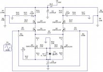
I've been working on a current-sourced and cascoded version of the Pass Balanced Line Stage. Attached is the circuit that I have been simulating. If anyone sees anything that isn't right, or has any suggestions for improvement, please let me know!
R8/R9- will be pots, as suggested by Nelson Pass. I still am not sure what to look for when adjusting this value. I was watching the voltage across the MOSFETs and the signal on the gates of the cascodes and adjusting these values for the smallest voltage drop with a clean signal on the gate. I would really appreciate someone telling me what I should be looking for.
R16/R17- standard 600 ohm load. I will be driving an A75 with this, so I think that the actual load will be a little lower (if I remember correctly, the A75 in balanced mode is a little over half that value, something like 375 ohms/input)
R20/R21- Will be 100 ohm pots.
R22/R23- Current sensing resistors for adjusting R20/R21
R5- Will be 500 Ohm pot, for adjusting gain, if for no other reason than to match channels.
Attachments
Hi Steve,
Great job !
As you seem concerned with the noise issue, try to add a small film cap (10 nF) across the Zener D1, which generally tends to be a noisy device.
Tell us what you get in real life.
Cheers,
Great job !
As you seem concerned with the noise issue, try to add a small film cap (10 nF) across the Zener D1, which generally tends to be a noisy device.
Tell us what you get in real life.
Cheers,
François,
thanks for the thumbs up and the suggestion! So, I need a 10nF cap across that zener as well as the 4.7µf? Any other suggestions would be very much appreciated. Thanks again.
Steve
thanks for the thumbs up and the suggestion! So, I need a 10nF cap across that zener as well as the 4.7µf? Any other suggestions would be very much appreciated. Thanks again.
Steve
Steve,
Some suggestions. I should point out at that I have designed and built many amps, both FET and bipolar, no-feedback and high feedback. It is always interesting to me to see the different genres of circuits. Two in particular stand out - those that are based on or derived from op-amp architectures and those derived from valve circuits. The former tend to have multiple, complex device arrangements, usually bipolar and incorporate feedback. The latter tend to be spartan by comparison: very few active devices, lots of resistors, few capacitors, relatively high voltages and low or no feedback and often curiously symmetrical schematics.
I think both genres have method behind their madnesses but sometimes the learnings from one do not find their way into the other. My suggestions will attempt to do this. Of course, Nelson is in the best position to advise and I will expect him to correct my reasoning as appropriate.
1) Although the symmetry of the schematic is very appealing to our eyes the electrons won't give a wet slap about how nice it looks. So I would be careful to make sure the circuit works well even if not symmetrical and also ensure each side works well on its own rather than relying on the differential output to eliminate all distortions.
2) R8/R9 are establishing a fixed bias voltage for Q3 and Q4 that are in turn shielding Q1 and Q2 from Vd variations realtive to ground. I would always put capacitors across these resistors to reduce noise from +V from modulating the bias voltage, especially at high f. 10uF would be fine.
3) I assume the reason for adjusting the values of R8 and R9 is to set different Vdg voltages on Q1,Q2 to make sure their Cdg are closely matched. This tries to make sure the frequency response of each side is closely matched. It is very difficult in practice to find two FETs that have idential parameters (your simulation will probably assume this).
4) Why have FET current sources? FETs have much higher capacitance than equivalent power bipolars and so will not look as close to being "small signal open circuits".
5) Why use two current sources? This looks pretty but is unecessary. Why not use one source and feed to the sources of Q1,Q2 vi a pot. You could replace R5 with a 120-ohm pot with the current source feeding the wiper. Using a single current source will also increase the impedance. In the actual circuit you would need to use a small, high quality pot.
6) Why use FETs for Q3/Q4? A couple of high-speed bipolars will maintain better voltage control and introduce much less capacitance to the circuit. Furthermore, if you use bipolars it will remove the need for these mountainous rail voltages. +/- 50V is chosen, presumably, to reduce the affects of FET non-linear capacitance changes as the output voltage changes. Why not eliminate the problem at source? This voltage range is way more than you need for a pre-amp that needs to swing 2V. If you use bipolars you can use rails as low as +/-15V and still maintain the same bias conditions for Q1/Q2.
BAM
BAM,
Thanks for the suggestions.
I was going to add the capacitors to the gates, but wasn't sure if it was correct. Thanks for the verification. Do you have any suggestions for a bipolar current source? I know there are examples out there, but which would work the best? I like the idea of one current source too... I didn't know how to apply it to the fets without getting rid of r5. I will have to try the potentiometer. My reason for sticking with FETS has to do with my understanding at this point. I have read a lot on tubes, and FETS seem to be quite similar. Bipolars confuse me! That's the short answer. If you have some circuit examples to share with me, I would really appreciate it. Thanks again.
Steve
Steve,
Keep the 4u7 cap and add the film cap. Values are not critical. I use 100uF//10nF for my BJT/Led current source.
I agree with BAM concerning bipolar current sources. I've tested BJT/Mosfet CS, and I prefer BJT. Use a red led as voltage reference (1.6 V but you may want to check, 'cause it depend on the make - ie the technology). Take a look at the schematics I posted in your previous thread. All is there, except for the "famous" film cap. BJTs are MJE15030.
Last suggestion, try to reduce the negative rail. It won't degrade the behaviour of the design, but will drastically reduce power dissipation. It's easier to to with BJT/Led CS, since the voltage drop ensuring proper function ot the CS is much lower.
Cheers,
Icurrent sourced cascoded BLS schematic
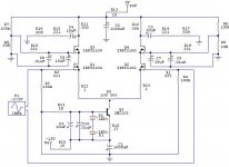
I like fet current sources and leave bipolars out of my designs. There seems to be quite a few who think all fet designs sound better. You can cascode the current sources for greater power supply rejection. Small cap across zener in addition to 4.7uF good idea.
H.H.
I like fet current sources and leave bipolars out of my designs. There seems to be quite a few who think all fet designs sound better. You can cascode the current sources for greater power supply rejection. Small cap across zener in addition to 4.7uF good idea.
H.H.
Hi back, Steve 😉
Some suggestions here.
I'll definitively go with two CS. One of the magic of the design is that you can simply trim the AC Gain with the source-to-source resistance. Now, what happens with the pot ? You will have to trim the pot value as well as the wiper position... In this case, you'd better replace the source resistances (R22/R23) with pots to adjust the gain. What do your simulations give at this point ?
Another thing is the negative rail. Be careful not to reduce it too much. The gate of the input mosfet is at 0V. So the source is 4-5 V below (ie -4V/-5V). Well, with two leds, you have about 3.5V across them, minus the Vbe ot the BJT, this leads to 2.8V across the emitter resistance. So, if neg rail is at -15 V, you have about -12.2 V at the emitter.
-12.2V down, -4/5V up, just 7/8V room left for the signal. Assume the input signal at +/-2V, on the most critical point, it leaves 5/6V between the mosfet source and BJT's emitter. It seriously reduces BJT's Vce, and I'm not quite sure that the current source is still that perfect (high impedance, linearity) at such low voltages. But it has to be tested 🙂
Steve,
Your revised schematic looks fine. I'm not sure of the characteristics of a 2N2102. Trannies like MJE243 or BD135 are definitely suitable.
"There seems to be quite a few who think all fet designs sound better"
Sounds like heresay/conjecture. Why should this be so? Use the right part for the job.
"you can simply trim the AC Gain with the source-to-source resistance"
True. You can still do with the single CCS by using a resistor in parallel with a higher value pot.
"it leaves 5/6V between the mosfet source and BJT's emitter"
Not an issue with a BJT. They are happy below 1V Vce. Unlike a FET.
BAM
OK, some answers as to the why here:
For the low voltage on the negative rail- I looked at the dissipation of the current source transistor, and it is at about 1/2 watt. Going up (down?) to -20 volts, and it is dissipating about 1.28 watts. The transistor was chosen because the simulation package I was using had this model, and it was rated a 1 watt, 1 amp. I am definitely open to other transistors. I was just using what I had to work with in my freeware 🙂(you gotta love freeware)
François, you have some interesting points about the voltage across the transistor. I will definitely have to look into that. Do you know of a way to get the dissipation down and the voltage up? The simulator is saying that this circuit the way it is will swing +/- 18V on each output into a 600 ohm load (wouldn't that be a 36 volts differentially?!!) with +/- 9.25 volts at each input at the onset of clipping. I know, I know... don't trust the simulator, ha ha. But that does seem pretty darn good. Thanks again for all the suggestions. Maybe when I get around to building this thing I will try a few different versions and see what the sound difference is. I'm open to any other suggestions, so please keep them coming. I surely don't mind a little critique.
Steve
Sorry, I missed something. In your schematic the decoupling capacitors for Q3, Q4 should be on the R8, R9 side of the gate resistors. Those gate resistors are there to damp HF energy so the FETs want to see a resistance on their gates rather than a short to ground. You don't really need two pairs of caps if you use good quality caps in the real circuit. So a 1uF or greater polypropylene will do on each side.
Steve,
The voltage drop 'cross the BJT seems to be fine according to BAM. But an old protecting and overkilling reflex led me to provide some "voltage space" to the design. I haven't had the time to really check my books, but once more I suspect that the current source behaviour is not as good as needed when the BJT's Vce is getting low. But maybe I'm completely wrong and I just want to learn...
Regarding dissipation in the BJT, you can fairly use a power BJT. Note that a side effect of using two CS is a way to reduce the dissipation (not the global one 🙂 but each transistor has half less power to withstand).
Cheers

Re: Show us your **ts (fets...... of course)
Hmmmmm..........looks a lot like John Curl fixing to smack Mark Levinson upside the head for stiffing him on his last royalty check.
As for using bipolars.........."What is the law?"
Bandwidth-limit the input signal.
Hmmmmm..........looks a lot like John Curl fixing to smack Mark Levinson upside the head for stiffing him on his last royalty check.
As for using bipolars.........."What is the law?"
Bandwidth-limit the input signal.

Where is the balance?
I have been messing around with this circuit a little more, and I find that the more I increase the bias current (using a source instead of the resistors), the less headroom I end up with.
Correct me if I'm wrong here:
using the original BLS circuit altered in the following ways:
Current sourced at 80mA per side. Load resistors lowered to 220 ohms. Gain-setting resistor lowered to approx. 150 ohms. Voltage rails at ±40V
Correct me if I'm wrong here:
The dc voltage measured at the MOSFET/load resistor junction should be 1/2 supply voltage for maximum voltage swing. With this combination of load resistor I am getting approx. 20 volts (1/2 of the 40V supply) at this point.
The gain seems to be set to about 3 using the resistors mentioned above.
The circuit is clipping quite a bit earlier than the normal BLS with lower current and a higher value load resistor. I assume that this is what should happen. My question now is how much headroom is needed? My SACD player claims to put out 2Vrms. This would be 5.656 volts input p-p. Is this the maximum it will see? Is the higher current worth getting less headroom out of the circuit? I assume from what I have read in Nelson's articles that it lowers the distortion. I believe that this is what is going on when the rail voltages are increased in the original circuit- the bias voltage relationship stays the same proportionally, but the current through the whole circuit is increased.
Do I now need to increase the upper rail voltage and go to a higher power MOSFET? This seems like it wouldn't be beneficial, as the higher powered MOSFET would produce more distortion, which would negate the effect of increasing the bias current.
Is the cascode the better way to go, with a similar amount of bias current to the original circuit? So many questions. Can anyone point me inthe right direction?
Thanks,
Steve
Keeping the bias current unchanged, increase both the positive voltage rail and the drain resistor, keeping the voltage drop across this resistor at Vsup/2. For instance, Ibias=80mA, Vsup=80V, Vsup/2=40V, Rdrain=500 Ohms. Don't forget to ensure proper wattage for these resistances (3.2W here)
The output swing is directly connected to this resistance : the same current variation will lead to a higher swing if the resistor is increased.
Oh, and I don't think you need to change the mosfets. Just heatsink them properly and they will do a nice job.
Hope this helps
The output swing is directly connected to this resistance : the same current variation will lead to a higher swing if the resistor is increased.
Oh, and I don't think you need to change the mosfets. Just heatsink them properly and they will do a nice job.
Hope this helps
- Status
- Not open for further replies.
- Home
- Amplifiers
- Pass Labs
- current sourced cascoded BLS schematic