mikeks said:Hi Jocko,
i see Nelson has retired your mate: Fred Deickman.....
😀
Exqueeze me?
Congrats......Professor!
I think that is safe to say that you have now confused the entire forum.
But what do I know? (Obviously, nothing, right?)
Jocko
I think that is safe to say that you have now confused the entire forum.
But what do I know? (Obviously, nothing, right?)
Jocko
Sorry Jocko,
But I do not know of someone named Fred Deickman ???
A search on that name didn’t bring up a member of this board with that name.
🙄
But I do not know of someone named Fred Deickman ???
A search on that name didn’t bring up a member of this board with that name.
🙄
Re: Re: Re: Re: Re: Re: Re: let us come to the point
Voltage stimulus is applied to the emitter of a common base stage with respect to its base...
Viz: You still have to vary the CB's emitter-base voltage to generate a change in its collector current, and hence collector voltage.....
Ultima Thule said:
How about a CB transistor stage?
Current in - voltage out, right!?
Cheers! 😉
Voltage stimulus is applied to the emitter of a common base stage with respect to its base...
Viz: You still have to vary the CB's emitter-base voltage to generate a change in its collector current, and hence collector voltage.....
Re: Re: Re: Re: Re: Re: Re: Re: let us come to the point
...ok, but how about my question in this post, I at least didn't ignore anything! 😎
mikeks said:
Voltage stimulus is applied to the emitter of a common base stage with respect to its base...
Viz: You still have to vary the CB's emitter-base voltage to generate a change in its collector current, and hence collector voltage.....
...ok, but how about my question in this post, I at least didn't ignore anything! 😎
Re: Re: Moreover..
...a so-called 'CFB' input stage....
....better defined as a low impedance voltage (LIV) feedback input stage...
...the extraordinary thing about this fuss is the fact that the so called 'current' feedback top[ology is merely an extension of the complementary feedback, (or sziklai), pair...
...which everyone here agrees is infact a case of voltage feedback....
...the term 'current feedback' was merely hijacked by the marketing mafiosi.....
Ultima Thule said:
Mike,
http://www.anasoft.co.uk/EE/currentfeedbackmyth/currentfeedbackmyth.html
do you agree with the whole content of that page, eg. that the mentioned/drawed CFB schematic is a CFB amplifier topology?
Cheers 😉
...a so-called 'CFB' input stage....
....better defined as a low impedance voltage (LIV) feedback input stage...
...the extraordinary thing about this fuss is the fact that the so called 'current' feedback top[ology is merely an extension of the complementary feedback, (or sziklai), pair...
...which everyone here agrees is infact a case of voltage feedback....
...the term 'current feedback' was merely hijacked by the marketing mafiosi.....
cfb error signal is current
Dear friends,
It seems that the term "current" feedback, or CFB, can really stir the pot of controversy. Back in the '80's when I first encountered the CFB topology, I must admit that it took some time for me to get used to it. I was so locked into "voltage" mode thinking that I was really fascinated by this current mode approach. Let's step through the CFB op-amp (CFA) and examine what happens in steady state as well as transient conditions. It will become apparent that in a CFA, the error signal that the output drives to zero is indeed a CURRENT, the difference between the first stage emitter currents, which is the current entering or exiting the inverting input terminal, or "neg" terminal. I have a zipped up archive of app notes, and the paper from Dr.Cherry which I can e-mail to any interested parties.
We have a CFA, with Rfb = 1.0 kohm = Rin. The pos input is driven by 0.50 V. The neg input is also at 0.50 V, since the input terminals of an op amp are at the same potential in steady state conditions (this holds for CFB and VFB op-amps). The closed loop gain is (1 + Rfb/Rin) = 2 in this case. The output is at 1.0 V. The current in Rfb, Irfb, is (Vout - Vn)/Rfb = (1.0 - 0.5)/(1.0) = 0.5 mA, where Vn is the voltage at the neg terminal, and Vout is the voltage at the op-amp output. Likewise, the current in Rin,Irin, is (Vn - 0)/Rin = (0.5)/(1.0) = 0.5 mA. The two currents are equal, and their difference is zero. The diference current is precisely equal to the current entering or leaving the neg input termainal, which we will call In. Under static or steady state conditions , In = 0, so that no current goes in or out of the neg input terminal. Although this terminal is a relatively low impedance, the current is zero for static conditions. Hence we can think of this terminal as a *"virtual"* open. The pos terminal voltage, Vp, equals the neg terminal voltage Vn, 0.50 V, although the pos input is a very high impedance. This is a "virtual" short condition, just like in a VFA. The "modus operandi" for a CFA, however, differs from a VFA. In a CFA, it is the input buffer, operating as an emitter follower, that forces Vn to equal Vp. The posiitve input Vp, is the buffer's input, with the neg input Vn, the buffer's output. It is this first stage buffer that forces Vn to follow Vp, NOT the output feedback action. This is extremely important. Despite minority opinion, the output voltage and the feedback network DO NOT drive the neg input voltage to equal the pos input voltage. The first stage buffer does that function.
Now let us perturb the input, by increasing the pos terminal input voltage from 0.50 to 1.0 V. The output will eventually reach 2.0 V, but it hasn't started moving yet (finite slew rate). What happens now? The pos input Vp, is at 1.0 V, the neg input Vn, is still at 0.50 V, Irfb = 0.50 mA = Irin, and Vout is still at 1.0 V. Because Vp is greater than Vn, the forward amplifier will drive the output upward. This does take time. Before that can happen, the input EF buffer drives the neg input Vn upward towards 1.0 V in order to follow pos input Vp. This will happen much quicker than the output changing because the input buffer is a single stage emitter follower, a very fast topology, least affected by Miller capacitance bottlenecking. Again, for emphasis, the EF input buffer stage immediately responds to the step change input at Vp and drives Vn to equal Vp, 1.0 V in this example. Now we have Vp = 1.0 V = Vn, so that Irin is now Vn/Rin = 1.0/1.0 = 1.0 mA. However with Vout = 1.0 V and Vn = 1.0 V, Rfb = (1.0 - 1.0)/ 1.0 = 0 mA. Since zero current flows in Rfb and 1.0 mA flows in Irin, the difference is now sourced by the neg input terminal. This current, In, is the difference between the currents in the feedback resistor pair. The upper transistor in the complementary pair EF sources this current, while the lower bjt sinks zero current Both bjt's currents are then MIRRORED over to the next stage. The DIFFERENCE of these reflected currents is fed into a grounded compensation capacitor. This capacitor current Ic is very nearly equal to In, the neg input terminal current which is the difference in the feedback resistor pair currents. The current Ic feeding the comp cap will increase the voltage on said cap forcing the output stage to slew the output voltage upward at its maximum rate. The comp cap and the associated output buffer stage form a *transimpedance* stage. A moment later, let's say the output voltage, Vout, is at 1.5 V. Now, Irfb = (1.5 - 1.0)/1.0 = 0.5 mA. With Irfb at 0.5 mA, and Irin at 1.0 mA, the difference current, In, is 0.5 mA, which is sourced from the neg input terminal. This current is mirrored over to the comp cap which continues to charge upward, but at a slower rate than before. The output voltage continues slewing upward, at this slower rate. Meanwhile the neg input terminal voltage remains at 1.0 V, equal to the pos input terminal voltage due to the EF input buffer. Now the output reaches 1.9 V. Then Rfb = (1.9 - 1.0)/1.0 = 0.9 mA, so that In = 1.0 - 0.9 = 0.1 mA. The comp cap is still charging, but at an even slower rate, which still drives the output voltage upward. When the output reaches exactly 2.0 V, then Irfb = (2.0 - 1.0)/1.0 or 1.0 mA, the exact same value as Irin. The difference current is now 1.0 - 1.0 = 0 mA. The zero current difference gets mirrored to the comp cap and the voltage on the cap remains unchanged, since no current is entering it. The output voltage now holds at 2.0 V, the final value. The output slews whenever In is non-zero, and stops at its final value when In is driven to zero. Thus In, the difference current, is the ERROR SIGNAL in this servo control loop. What happens next if the loop is underdamped and Vout overshoots to 2.1 V? The Rfb current Irfb is (2.1 - 1.0)/1.0 = 1.1 mA, with Irin still at 1.0 mA. The difference is -0.1 mA which the neg input terminal must now SINK. This neg sink current is mirrored over to the comp cap and DISCHARGES it. The output voltage turns around and slews DOWNWARD. When the output reaches 2.0 V, both resistors have 1.0 mA, and the error signal, In, is zero. The output settles at 2.0 V.
To summarize a CFA servo action, an inequality in feedback resistor currents causes the EF first stage (neg input terminal) bjt's to source or sink the difference in these currents. This difference, due to the current mirrors, is reflected to the comp cap and output buffer, which form a transimpedance stage which drives the output voltage in the direction forced by the error signal current. The output voltage will slew until the error signal current is driven to zero. The terminology "current feedback" is precisely correct. The input terminal voltage difference is forced to zero, not by the overall feedback loop, but by the first stage input buffer, operating in emitter follower mode.
Anyway, let me revisit what CFB-terminology critic Dr. Cherry wrote in his paper, discussed here often.
On p337-338, he writes:
"Stripped of its input level shifters and complementary first stage, and with the current mirrors and voltage follower replaced by the simplest inverting amplifier (a single common-emitter transistor), the current-feedback amplifier reduces to Fig. 6. A generation ago this circuit was called a voltage-feedback pair. It differs from Fig. 2a only in that the current flowing into the left-hand side of the feedback network is the input current multiplied by the gain of the first transistor, as distinct from the input current itself."
Folks, the very parts he wishes to "strip", are exactly the parts which make the CFA uniquely different from the VFA. If the EF and current mirrors are replaced with a common-emitter (CE) amplifier, OF COURSE it reduces to a VFA. In a CFA the EF forces Vn to equal Vp, whereas in a VFA the output voltage and feedback network do this. In a CFA the current mirrors reflect the current difference in the feedback resistor pair over to the transimpedance stage, and charge up the comp cap, driving the output voltage in proportion to the difference CURRENT! Without the parts Dr. Cherry wishes to strip, the error signal becomes the voltage difference between Vn and Vp. A VFA is all that remains. You can't just remove critical parts at will, and then claim that this circuit is just like any other! If I were to clip all of the feathers off of both wings of a bird, does that "prove" that a bird doesn't really fly, and that it is just another land animal?
Just to review let's look at a VFA with Rfb = Rin = 1.0 kohm, Vin = Vp = 0.50 V. Of course, Vn = 0.50 V, and Vout = 1.0 V. Now raise Vin = Vp to 1.0 V. Vn remains at 0.50 V, and Vout is still 1.0 V. The voltage difference between the pos and neg input terminals Vp and Vn was originally 0 V, a "virtual" short, but is now 0.5 V, with Vp LARGER than Vn. This voltage difference is amplified by the forward gain and the output voltage slews UPWARD. As the output voltage rises, the voltage on the neg input terminal, Vn, rises, since Vin = 0.5* Vout. As long as Vp and Vn differ, the difference is amplified and Vout slews. When Vout reaches its final value of 2.0 V, the neg input, Vn is at 0.5*2.0 or 1.0 V, equalling the pos input Vp. The difference voltage between the two inputs has been driven to zero. Thus the error signal in a VFA if the input terminals voltage difference. Should Vout overshoot to 2.1 V, Vn now equals 1.05 V with Vp at 1.0 V. The 0.05 volt difference gets amplified. Since Vp is SMALLER than Vn, the output slews DOWNWARD. At Vout = 2.0 V, Vp - Vn = 0, and the output holds its value.
It is quite apparent that a CFA is NOT a low-Z VFA.
I'll continue in my next post. Best wishes.
cfb continued
Regarding bandwidth, BW, the CFA output slews at a rate proportional to the differential current. In the CFA step response above, the voltage across Rin is driven by the input buffer, Vn, and current is present in Rin. The current in Rfb is driven by the difference between Vout and Vn. The slew rate that the output can attain is dictated by the amount of current charging the comp cap. If the 1.0 kohm resistor pair was replaced with a 2.0 kohm pair, only half of the current would be available to charge the comp cap. The speed would be cut in half. The voltages remain the same but the current decreased, causing the speed to decrease. In a CFA, speed is proportional to current. Lower valued resistors result in higher speed. If the closed loop gain is increased by reducing the input resistor, holding the same value of feedback resistor, the slew rate remains unchanged. At unity gain, Rfb = 1.0 kohm, Rin = open. Letting the input at Vp increase from 0.5 to 1.0 volts, Vn is driven to 1,0 volts by the input EF buffer. A current of 0.5 mA flows from the negative input towards the output. The 0.5 mA is mirrored and charges the comp cap, and the output slews from 0.5 to 1.0 volts. Now let Rin = 1.0 kohm, for a closed loop gain of 2. The same step change in input from 0.5 to 1.0 volts produces a difference current of 1.0 mA, slewing the output from 1.0 to 2.0 volts. The difference current and the output voltage step change both double. There is no loss of speed at the higher gain value. The feedback voltage changed but BW remains the same.
With the VFA, it is the fed back voltage which forces the output stage compensating cap to charge and slew the output voltage. With unity gain, a voltage follower, the closed loop gain is 1, and the feedback factor is 100 percent or 1. When the input is suddenly changed, a voltage difference is created between Vp and Vn. This is the error signal which drives the output. Since the feedback factor is 1, all of the output voltage drives Vn, causing the output stage to slew the output voltage upward at its maximum rate. With the same VFA whose closed loop gain is increased to 2, the feedback factor is 50%, or 0.50. When the input is changed, only HALF of the output voltage drives Vn. The comp cap is charged at only half the rate, and the speed is halved. Decreasing the value of the feedback resistors does nothing, since it is the feedback VOLTAGE ratio that dictates the slew rate.
As far as BW goes, like most circuit designers, I aim for a nice comfortable stability margin (gain and phase), while trying to obtain as much speed as I can *safely* get. With a fast VFA, if I compensate for sufficient stability at unity gain, I can get high speed, or BW, maybe even comparable to a CFA. If, however, I need to set the gain for 2 for a specific circuit, using the same compensation, I am now over-compensated. My stability margin is excessive, at the price of reduced speed. I could, however redesign the comp network for sufficient stability at gain of 2, and enjoy more BW. I cannot then use this comp scheme at unity gain, or stability will be lost. If my application requires an amp that can be used over a wide range of gains, I am stuck. Or with auto-gain control circuits, I must compensate for the lowest anticipated gain, and accept reduced BW at higher gains.
It would be great if I could have both BW and stability at all gains. With unity gain compensation in a VFA, if I increase the gain to 2, the feedback factor beta decreases to 0.5. The open loop gain remains the same, while beta decreases to half. The product of open loop gain and beta is the *loop gain*. The optimum condition would be to have a steady loop gain. As beta increases, open loop gain would decrease, holding loop gain steady. This would provide sufficient, but not excessive stability margin over a wide range of gains, while preserving full BW. A CFA provides exactly this feature. Dr. Cherry acknowledges this on p. 338 bottom right, only he was referring to the transconductance feedback amp topology:
"The feedback resistors are the only load on the current-gain amplifier, so forward path voltage gain is directly proportional to these resistors. Hence loop gain remains constant if demanded gain is changed by varying Rf2 at constant Rf1."
With a CFA, as the beta (feedback factor) decreases, the open loop gain goes up, and loop gain remains constant. Decreasing beta coincides with higher closed loop gain. Since loop gain does not degrade with higher closed loop gains, one compensation scheme can provide sufficient, but not excessive stability margins, AND nearly full bandwidth capability, over a WIDE RANGE of closed loop gains. With a VFA, any one set of compensating values will produce sufficient stability and full bandwidth over a NARROW RANGE of closed loop gains. At lower closed loop gain values, instability looms large, and at higher gains, speed is greatly reduced.
I hope that this treatise has made CFA's a little easier to understand. In order to fully comprehend, one should start with an example, inputting a specific voltage, computing the resulting quantities, and then input a step change. Then compute the results, and observe. Without actually doing this, it is quite difficult to gain understanding merely by inspection or "arm-waving". Those who wish to diss this treatise should put their money where their mouth is, and offer a step by step mathematical example, covering in detail the operation of a CFA. Otherwise, they don't really know it as well as they think. Best wishes.
Re: cfb error signal is current
great post, well written.
I just not sure if the points would be understood. The same thing (the error signal in a cfa is current) was said very early in their threads (someone did it and I followed up as well).
And count-less posts later we are at the exact same place.
It is futile to resist the borg. It is equally futile to debate with people who refuse to listen.
Claude Abraham said:Dear friends,
I'll continue in my next post. Best wishes.
great post, well written.
I just not sure if the points would be understood. The same thing (the error signal in a cfa is current) was said very early in their threads (someone did it and I followed up as well).
And count-less posts later we are at the exact same place.
It is futile to resist the borg. It is equally futile to debate with people who refuse to listen.
Well done, Claude.....
Let's give this guy some kinf of award.......
Using Cherry's "logic", I guess that we could then say:
"A modern automotive vehicle, stripped of its drivetrain, reduces to nothing more than a glorified 2-ton soap box derby racer."
Jocko
Let's give this guy some kinf of award.......
Using Cherry's "logic", I guess that we could then say:
"A modern automotive vehicle, stripped of its drivetrain, reduces to nothing more than a glorified 2-ton soap box derby racer."
Jocko
Re: Well done, Claude.....
or:
"human, stripped of its intelligence, is nothing but a collection of carbon, oxygen and hydrogen atoms, save a few others".
Maybe we should just strike out the word "human" from our dictionary and use COH atoms instead?
🙂
Jocko Homo said:Using Cherry's "logic", I guess that we could then say:
"A modern automotive vehicle, stripped of its drivetrain, reduces to nothing more than a glorified 2-ton soap box derby racer."
Jocko
or:
"human, stripped of its intelligence, is nothing but a collection of carbon, oxygen and hydrogen atoms, save a few others".
Maybe we should just strike out the word "human" from our dictionary and use COH atoms instead?
🙂
Pjotr said:Sorry Jocko,
But I do not know of someone named Fred Deickman ???
A search on that name didn’t bring up a member of this board with that name.
🙄
....probably because his name actually is Fred Dieck man....
Re: cfb error signal is current
Dear Claude,
Thank you for this most interesting treatise on this vexatious issue.
You have self-evidently cogitated and ruminated at some considerable length on the subject.
While your effort deserves no less than a line by line response to do it justice, i shall presently confine my rebuttal to the following excerpt.
This is reasonable, as this ineffably flawed extract constitutes the cornerstone of your position.
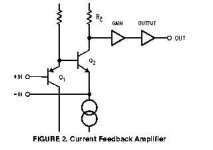
If this were true, then it might quite reasonably be applied to the generic voltage feedback topology shown below.
For it could then be urgued that the error signal driving the foward path is a current, being effectively the difference between Q2 and Q4's collector current.
This may at first appear true as this 'error' current is directly proportional to the voltage vd, further downstream.
But is vastly incorrect because this current merely represents an effect, with the causal error signal being the differential voltage vd.
Therefore, for both topologies it is clear that the error signal resolutely remains a voltage. viz. The difference between input and feedback voltages.
That this error voltage is subsequently expressed as a current downstream is of secondary significance.
Dear Claude,
Thank you for this most interesting treatise on this vexatious issue.
You have self-evidently cogitated and ruminated at some considerable length on the subject.
While your effort deserves no less than a line by line response to do it justice, i shall presently confine my rebuttal to the following excerpt.
This is reasonable, as this ineffably flawed extract constitutes the cornerstone of your position.
Claude Abraham said:
.........It will become apparent that in a CFA, the error signal that the output drives to zero is indeed a CURRENT, the difference between the first stage emitter currents, which is the current entering or exiting the inverting input terminal, or "neg" terminal.
If this were true, then it might quite reasonably be applied to the generic voltage feedback topology shown below.
For it could then be urgued that the error signal driving the foward path is a current, being effectively the difference between Q2 and Q4's collector current.
This may at first appear true as this 'error' current is directly proportional to the voltage vd, further downstream.
But is vastly incorrect because this current merely represents an effect, with the causal error signal being the differential voltage vd.
Therefore, for both topologies it is clear that the error signal resolutely remains a voltage. viz. The difference between input and feedback voltages.
That this error voltage is subsequently expressed as a current downstream is of secondary significance.
Attachments
Re: cfb error signal is current
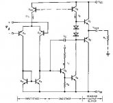
This is incorrect...Dr. Cherry was right in all respects. See figure below obtained from:
http://www.national.com/an/AN/AN-597.pdf
Claude Abraham said:..........Anyway, let me revisit what CFB-terminology critic Dr. Cherry wrote in his paper, discussed here often.
On p337-338, he writes:
"Stripped of its input level shifters and complementary first stage, and with the current mirrors and voltage follower replaced by the simplest inverting amplifier (a single common-emitter transistor), the current-feedback amplifier reduces to Fig. 6. A generation ago this circuit was called a voltage-feedback pair. It differs from Fig. 2a only in that the current flowing into the left-hand side of the feedback network is the input current multiplied by the gain of the first transistor, as distinct from the input current itself."
Folks, the very parts he wishes to "strip", are exactly the parts which make the CFA uniquely different from the VFA. If the EF and current mirrors are replaced with a common-emitter (CE) amplifier, OF COURSE it reduces to a VFA. In a CFA the EF forces Vn to equal Vp, whereas in a VFA the output voltage and feedback network do this. In a CFA the current mirrors reflect the current difference in the feedback resistor pair over to the transimpedance stage, and charge up the comp cap, driving the output voltage in proportion to the difference CURRENT! Without the parts Dr. Cherry wishes to strip, the error signal becomes the voltage difference between Vn and Vp. A VFA is all that remains. You can't just remove critical parts at will, and then claim that this circuit is just like any other! If I were to clip all of the feathers off of both wings of a bird, does that "prove" that a bird doesn't really fly, and that it is just another land animal?
This is incorrect...Dr. Cherry was right in all respects. See figure below obtained from:
http://www.national.com/an/AN/AN-597.pdf
Attachments
I'm sorry!
I'm using orcad 9.2 .How can I do to calculate open-loop BW of a amp?
How can I do to have a amp have open-loop BW is 25khz?🙂
I'm using orcad 9.2 .How can I do to calculate open-loop BW of a amp?
How can I do to have a amp have open-loop BW is 25khz?🙂
Re: cfb error signal is current
No....the output of an amplifier of whatever complexion does not...and cannot drive the error signal to zero....for obvious reasons.... 🙂
Claude Abraham said:
.......the error signal that the output drives to zero ......
No....the output of an amplifier of whatever complexion does not...and cannot drive the error signal to zero....for obvious reasons.... 🙂
thanh said:How can I do to have a amp have open-loop BW is 25khz?🙂
Thanh...if you give me just one good reason why you need an amplifier with a forward-path bandwidth of 25KHz, i'll design one for you in a separate thread inside two minutes....
In my view there is no earthly reason why this is desirable....
Re: Re: cfb error signal is current
For the same you can state:
“But is vastly incorrect because this voltage merely represents an effect, with the causal error signal being the differential current”
But this way of looking does not seem to exist in your world Mike.
It amazes me time after time that a lot of EE’s (not to say the majority) tend to convert everything they encounter into voltages, even when currents are more appropriate. Seems they can’t live with currents. They once started with a battery in their early life that had a specific voltage and their whole life they stay referencing anything to that early battery.
Cheers 😉
mikeks said:But is vastly incorrect because this current merely represents an effect, with the causal error signal being the differential voltage vd..
For the same you can state:
“But is vastly incorrect because this voltage merely represents an effect, with the causal error signal being the differential current”
But this way of looking does not seem to exist in your world Mike.
It amazes me time after time that a lot of EE’s (not to say the majority) tend to convert everything they encounter into voltages, even when currents are more appropriate. Seems they can’t live with currents. They once started with a battery in their early life that had a specific voltage and their whole life they stay referencing anything to that early battery.
Cheers 😉
People forget that a bipolar transistor is actually a voltage controlled device, with a mathematically precise exponential Ic/Vb transfer function that holds over many decades.
To treat a bipolar transistor as a current controlled Ic/Ib device is a crude approximation.
Not that this affects the analysis of a CFB amp in any way. As Claude has said, the basic error signal in a CFB amp is a current, and now matter how much Mike blusters, his is a lone voice crying out against engineering orthodoxy.
I do agree that the term CFB was perhaps poorly chosen, when it (sometimes and erroneously) had in the past been used to describe feedback where the feedback VOLTAGE was derived by passing the output current through a resistor and measuring the VOLTAGE across the resistor.
- Status
- Not open for further replies.
- Home
- Amplifiers
- Solid State
- Current feedback - Voltage feedback, how do I see the difference?